JAJSGA2F September 2018 – June 2021 TPS2663
PRODUCTION DATA
- 1 特長
- 2 アプリケーション
- 3 概要
- 4 Revision History
- 5 Device Comparison Table
- 6 Pin Configuration and Functions
- 7 Specifications
- 8 Parameter Measurement Information
-
9 Detailed Description
- 9.1 Overview
- 9.2 Functional Block Diagram
- 9.3
Feature Description
- 9.3.1 Hot Plug-In and In-Rush Current Control
- 9.3.2 PGOOD and PGTH
- 9.3.3 Undervoltage Lockout (UVLO)
- 9.3.4 Overvoltage Protection (OVP)
- 9.3.5 Input Reverse Polarity Protection (B_GATE, DRV)
- 9.3.6 Reverse Current Protection
- 9.3.7 Overload and Short Circuit Protection
- 9.3.8 Output Power Limiting, PLIM (TPS26632, TPS26633, TPS26635 and TPS26636 Only)
- 9.3.9 Current Monitoring Output (IMON)
- 9.3.10 FAULT Response ( FLT)
- 9.3.11 IN_SYS, IN, OUT and GND Pins
- 9.3.12 Thermal Shutdown
- 9.3.13 Low Current Shutdown Control (SHDN)
- 9.4 Device Functional Modes
-
10Application and Implementation
- 10.1 Application Information
- 10.2
Typical Application: Power Path Protection in a PLC System
- 10.2.1 Design Requirements
- 10.2.2 Detailed Design Procedure
- 10.2.3 Application Curves
- 10.3 System Examples
- 10.4 Do's and Don'ts
- 11Power Supply Recommendations
- 12Layout
- 13Device and Documentation Support
- 14Mechanical, Packaging, and Orderable Information
9.3.7.1.2 Active Current Limiting with 2x IOL Pulse Current Support, (TPS26631, TPS26633, TPS26635 and TPS26636 Only)
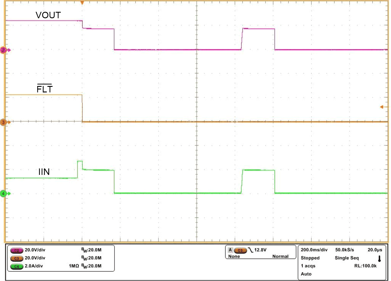
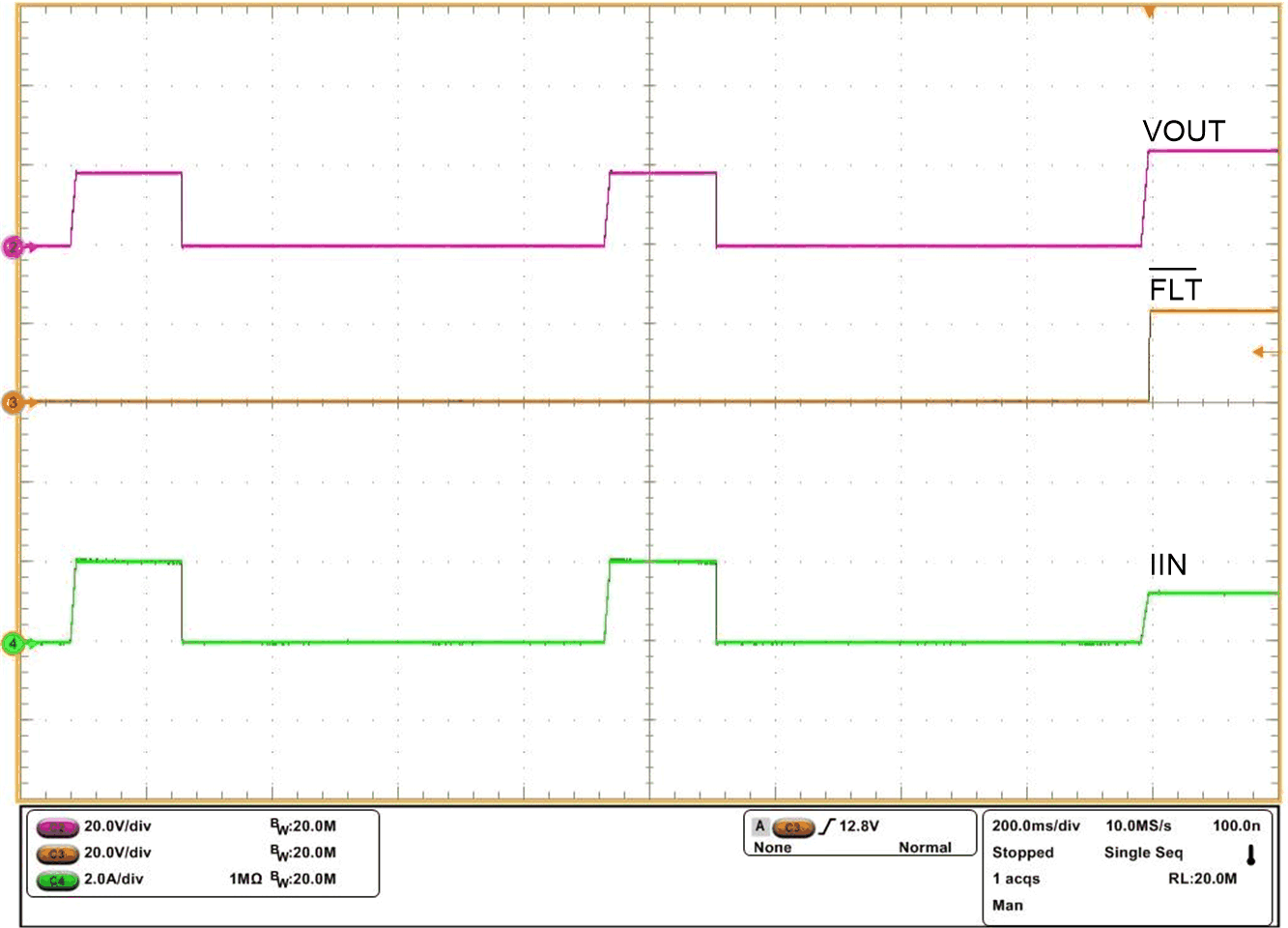
TPS26631,TPS26633,TPS26635 and TPS26636 after the start-up and with PGOOD high, if the load current exceeds IOL, then an internal fixed tCB(dly), 25.5 msec (typical) timer starts. During this time the device will pass through the over current demanded by the load not more than 2 x IOL above which the device will regulate at 2 x IOL. After tCB(dly) time, the device regulates the current at IOL. The power dissipation across the device during this operation will be (VIN–VOUT) x IOL and this could heat up the device and eventually enter into thermal shutdown. The maximum duration for the internal FET in current regulation is tCL_PLIM(dly). The subsequent operation will be based on the MODE setting (either auto-retry or latch OFF) in Table 9-1.
The 2 x I(OL) pulse current support is activated only after PGOOD goes high. If PGOOD is in low state such as during start-up operation or during auto-retry cycles, the 2 x I(OL) pulse current support is not activated and the device limits the current at I(OL) level.
Figure 9-12 and Figure 9-13 illustrate overload current limiting performance.

| VIN_SYS = 24 V | MODE connected to GND (Auto-Retry) | RILIM = 9 kΩ |

| VIN_SYS = 24 V | MODE connected to GND (Auto-Retry) | RILIM = 9 kΩ |
The TPS2663x devices feature ILIM pin short and open fault detection and protection. The internal FET is turned OFF when ILIM pin is detected short or open to GND and it remains OFF till the ILIM pin fault is removed.
Refer to Figure 8-2 for more information on tCB(dly) and tCL_PLIM(dly) parameter measurement information.