JAJSJT8C May 2020 – June 2021 TPS543620
PRODUCTION DATA
- 1 特長
- 2 アプリケーション
- 3 概要
- 4 Revision History
- 5 Pin Configuration and Functions
- 6 Specifications
-
7 Detailed Description
- 7.1 Overview
- 7.2 Functional Block Diagram
- 7.3
Feature Description
- 7.3.1 VIN Pins and VIN UVLO
- 7.3.2 Enable and Adjustable UVLO
- 7.3.3 Adjusting the Output Voltage
- 7.3.4 Switching Frequency Selection
- 7.3.5 Switching Frequency Synchronization to an External Clock
- 7.3.6 Ramp Amplitude Selection
- 7.3.7 Soft Start and Prebiased Output Start-up
- 7.3.8 Mode Pin
- 7.3.9 Power Good (PGOOD)
- 7.3.10 Current Protection
- 7.3.11 Output Overvoltage and Undervoltage Protection
- 7.3.12 Overtemperature Protection
- 7.3.13 Output Voltage Discharge
- 7.3.14 Low-Side MOSFET Resistance Scaling
- 7.4 Device Functional Modes
-
8 Application and Implementation
- 8.1 Application Information
- 8.2
Typical Applications
- 8.2.1
1.0-V Output, 1-MHz Application
- 8.2.1.1 Design Requirements
- 8.2.1.2
Detailed Design Procedure
- 8.2.1.2.1 Switching Frequency
- 8.2.1.2.2 Output Inductor Selection
- 8.2.1.2.3 Output Capacitor
- 8.2.1.2.4 Input Capacitor
- 8.2.1.2.5 Adjustable Undervoltage Lockout
- 8.2.1.2.6 Output Voltage Resistors Selection
- 8.2.1.2.7 Bootstrap Capacitor Selection
- 8.2.1.2.8 BP5 Capacitor Selection
- 8.2.1.2.9 PGOOD Pullup Resistor
- 8.2.1.2.10 Current Limit Selection
- 8.2.1.2.11 Soft-Start Time Selection
- 8.2.1.2.12 Ramp Selection and Control Loop Stability
- 8.2.1.2.13 MODE Pin
- 8.2.1.3 Application Curves
- 8.2.2 1.0-V Output, 1.5-MHz Application
- 8.2.3 3.3-V Output, 1.0-MHz Application
- 8.2.4 1.8-V Output, 1.0-MHz Typical Application
- 8.2.5 5.0-V Output, 1.0-MHz Typical Application
- 8.2.1
1.0-V Output, 1-MHz Application
- 9 Power Supply Recommendations
- 10Layout
- 11Device and Documentation Support
- 12Mechanical, Packaging, and Orderable Information
8.2.1.2.4 Input Capacitor
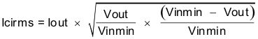
Input decoupling ceramic capacitors type X5R, X7R, or similar from VIN to PGND that are placed as close as possible to the IC are required. A total of at least 10 µF of capacitance is required and some applications can require a bulk capacitance. At least 1 µF of bypass capacitance is recommended as close as possible to each VIN pin to minimize the input voltage ripple. A 0.1-µF to 1-µF capacitor must be placed as close as possible to both VIN pins 8 and 12 on the same side of the board of the device to provide high frequency bypass to reduce the high frequency overshoot and undershoot on VIN and SW pins. The voltage rating of the input capacitor must be greater than the maximum input voltage. The capacitor must also have a ripple current rating greater than the maximum RMS input current. The RMS input current can be calculated using Equation 16.
For this example design, a ceramic capacitor with at least a 16-V voltage rating is required to support the maximum input voltage. Two 10-µF, 0805, X7S, 25-V and two 0.1-μF, 0402, X7R 50-V capacitors in parallel have been selected to be placed on both sides of the IC near both VIN pins to PGND pins. Based on the capacitor manufacturer's website, the total ceramic input capacitance derates to 5.4 µF at the nominal input voltage of 12 V. A 100-µF bulk capacitance is also used to bypass long leads when connected a lab bench top power supply.
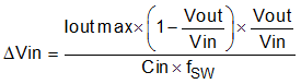
The input capacitance value determines the input ripple voltage of the regulator. The input voltage ripple can be calculated using Equation 17. The maximum input ripple occurs when operating nearest to 50% duty cycle. Using the nominal design example values of Ioutmax = 6 A, CIN = 5.4 μF, and fSW = 1000 kHz, the input voltage ripple with the 12 V nominal input is 85 mV and the RMS input ripple current with the 4.5 V minimum input is 4.9 A.