JAJSJT8C May 2020 – June 2021 TPS543620
PRODUCTION DATA
- 1 特長
- 2 アプリケーション
- 3 概要
- 4 Revision History
- 5 Pin Configuration and Functions
- 6 Specifications
-
7 Detailed Description
- 7.1 Overview
- 7.2 Functional Block Diagram
- 7.3
Feature Description
- 7.3.1 VIN Pins and VIN UVLO
- 7.3.2 Enable and Adjustable UVLO
- 7.3.3 Adjusting the Output Voltage
- 7.3.4 Switching Frequency Selection
- 7.3.5 Switching Frequency Synchronization to an External Clock
- 7.3.6 Ramp Amplitude Selection
- 7.3.7 Soft Start and Prebiased Output Start-up
- 7.3.8 Mode Pin
- 7.3.9 Power Good (PGOOD)
- 7.3.10 Current Protection
- 7.3.11 Output Overvoltage and Undervoltage Protection
- 7.3.12 Overtemperature Protection
- 7.3.13 Output Voltage Discharge
- 7.3.14 Low-Side MOSFET Resistance Scaling
- 7.4 Device Functional Modes
-
8 Application and Implementation
- 8.1 Application Information
- 8.2
Typical Applications
- 8.2.1
1.0-V Output, 1-MHz Application
- 8.2.1.1 Design Requirements
- 8.2.1.2
Detailed Design Procedure
- 8.2.1.2.1 Switching Frequency
- 8.2.1.2.2 Output Inductor Selection
- 8.2.1.2.3 Output Capacitor
- 8.2.1.2.4 Input Capacitor
- 8.2.1.2.5 Adjustable Undervoltage Lockout
- 8.2.1.2.6 Output Voltage Resistors Selection
- 8.2.1.2.7 Bootstrap Capacitor Selection
- 8.2.1.2.8 BP5 Capacitor Selection
- 8.2.1.2.9 PGOOD Pullup Resistor
- 8.2.1.2.10 Current Limit Selection
- 8.2.1.2.11 Soft-Start Time Selection
- 8.2.1.2.12 Ramp Selection and Control Loop Stability
- 8.2.1.2.13 MODE Pin
- 8.2.1.3 Application Curves
- 8.2.2 1.0-V Output, 1.5-MHz Application
- 8.2.3 3.3-V Output, 1.0-MHz Application
- 8.2.4 1.8-V Output, 1.0-MHz Typical Application
- 8.2.5 5.0-V Output, 1.0-MHz Typical Application
- 8.2.1
1.0-V Output, 1-MHz Application
- 9 Power Supply Recommendations
- 10Layout
- 11Device and Documentation Support
- 12Mechanical, Packaging, and Orderable Information
8.2.1.2.6 Output Voltage Resistors Selection
The output voltage is set with a resistor divider created by RFBT and RFBB from the output node to the FB pin. It is recommended to use 1% tolerance or better resistors. For this example design, 4.99 kΩ was selected for RFBB. Using Equation 18, RFBT is calculated as 4.99 kΩ. This is a standard 1% resistor.
Equation 18. 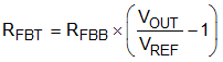
If the PCB layout does not use the recommended AGND to PGND connection in Section 10.1, noise on the feedback pin can degrade the output voltage regulation at max load. Use a smaller RFBB of 1.00 kΩ minimizes the impact of this noise.