JAJSJT8C May 2020 – June 2021 TPS543620
PRODUCTION DATA
- 1 特長
- 2 アプリケーション
- 3 概要
- 4 Revision History
- 5 Pin Configuration and Functions
- 6 Specifications
-
7 Detailed Description
- 7.1 Overview
- 7.2 Functional Block Diagram
- 7.3
Feature Description
- 7.3.1 VIN Pins and VIN UVLO
- 7.3.2 Enable and Adjustable UVLO
- 7.3.3 Adjusting the Output Voltage
- 7.3.4 Switching Frequency Selection
- 7.3.5 Switching Frequency Synchronization to an External Clock
- 7.3.6 Ramp Amplitude Selection
- 7.3.7 Soft Start and Prebiased Output Start-up
- 7.3.8 Mode Pin
- 7.3.9 Power Good (PGOOD)
- 7.3.10 Current Protection
- 7.3.11 Output Overvoltage and Undervoltage Protection
- 7.3.12 Overtemperature Protection
- 7.3.13 Output Voltage Discharge
- 7.3.14 Low-Side MOSFET Resistance Scaling
- 7.4 Device Functional Modes
-
8 Application and Implementation
- 8.1 Application Information
- 8.2
Typical Applications
- 8.2.1
1.0-V Output, 1-MHz Application
- 8.2.1.1 Design Requirements
- 8.2.1.2
Detailed Design Procedure
- 8.2.1.2.1 Switching Frequency
- 8.2.1.2.2 Output Inductor Selection
- 8.2.1.2.3 Output Capacitor
- 8.2.1.2.4 Input Capacitor
- 8.2.1.2.5 Adjustable Undervoltage Lockout
- 8.2.1.2.6 Output Voltage Resistors Selection
- 8.2.1.2.7 Bootstrap Capacitor Selection
- 8.2.1.2.8 BP5 Capacitor Selection
- 8.2.1.2.9 PGOOD Pullup Resistor
- 8.2.1.2.10 Current Limit Selection
- 8.2.1.2.11 Soft-Start Time Selection
- 8.2.1.2.12 Ramp Selection and Control Loop Stability
- 8.2.1.2.13 MODE Pin
- 8.2.1.3 Application Curves
- 8.2.2 1.0-V Output, 1.5-MHz Application
- 8.2.3 3.3-V Output, 1.0-MHz Application
- 8.2.4 1.8-V Output, 1.0-MHz Typical Application
- 8.2.5 5.0-V Output, 1.0-MHz Typical Application
- 8.2.1
1.0-V Output, 1-MHz Application
- 9 Power Supply Recommendations
- 10Layout
- 11Device and Documentation Support
- 12Mechanical, Packaging, and Orderable Information
7.3.2 Enable and Adjustable UVLO
The EN pin provides on/off control of the device. Once the EN pin voltage exceeds its threshold voltage, the device begins its start-up sequence. If the EN pin voltage is pulled below the threshold voltage, the regulator stops switching and enters a low operating current state. The EN pin has an internal pullup current source, Ip, allowing it to be floated to enable the device by default. It is important to ensure that leakage currents of anything connected to the EN pin do not exceed the minimum EN pullup current or the device may not be able to start. If an application requires controlling the EN pin, an open drain or open collector output logic can be interfaced with the pin.
When the EN pin voltage exceeds its threshold voltage and the VIN pin voltage exceeds its VIN UVLO threshold, the device begins its start-up sequence. First, the BP5 LDO is enabled and charges the external BP5 capacitor. Once the voltage on the BP5 pin exceeds its UVLO threshold, the device enters a power-on delay. During the power-on delay, the values of the pinstrap resistors on the MODE pin (see Section 7.3.8) and SYNC/FSEL pin (see Section 7.3.4) are determined and the control loop is initialized. The power-on delay is typically 600 μs. After the power-on delay, soft start begins.
 Figure 7-1 Start-up Sequence
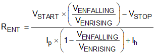
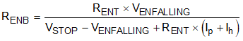
An external resistor divider can be added from VIN to the EN pin for adjustable UVLO and hysteresis as shown in Figure 7-2. The EN pin has a small pullup current, Ip, which sets the default state of the pin to enable when no external components are connected. The pullup current is also used to control the voltage hysteresis for the UVLO function since it increases by Ih once the EN pin crosses the enable threshold. The UVLO thresholds can be calculated using Equation 1 and Equation 2. When using the adjustable UVLO function, 500 mV or greater hysteresis is recommended. For applications with very slow input voltage slew rate, a capacitor can be placed from the EN pin to ground to filter any glitches on the input voltage.
 Figure 7-2 Adjustable UVLO Using EN