SGLS246B June 2004 – October 2016 TPS60400-Q1 , TPS60401-Q1 , TPS60402-Q1 , TPS60403-Q1
PRODUCTION DATA.
- 1 Features
- 2 Applications
- 3 Description
- 4 Revision History
- 5 Device Comparison Table
- 6 Pin Configuration and Functions
- 7 Specifications
- 8 Detailed Description
- 9 Application and Implementation
- 10Power Supply Recommendations
- 11Layout
- 12Device and Documentation Support
- 13Mechanical, Packaging, and Orderable Information
パッケージ・オプション
デバイスごとのパッケージ図は、PDF版データシートをご参照ください。
メカニカル・データ(パッケージ|ピン)
- DBV|5
サーマルパッド・メカニカル・データ
発注情報
1 Features
- Qualified for Automotive Applications
- AEC-Q100 Test Guidance With the Following Results:
- Device Temperature Grade 1: –40°C to +125°C Ambient Operating Temperature Range
- Device HBM ESD Classification Level 2
- Device CDM ESD Classification Level C6
- Inverts Input Supply Voltage
- Up to 60-mA Output Current
- Only Three Small 1-µF Ceramic Capacitors Needed
- Input Voltage Range From 1.8 V to 5.25 V
- PowerSave-Mode for Improved Efficiency at Low Output Currents (TPS60400-Q1)
- Device Quiescent Current Typical: 100 µA
- Integrated Active Schottky-Diode for Start-Up Into Load
- Small 5-Pin SOT23 Package
- Evaluation Module Available: TPS60400EVM-178
2 Applications
- Automotive Infotainment
- Automotive Cluster
- LCD Displays
- Negative Supply Voltages
3 Description
The TPS6040x-Q1 family of devices generate an unregulated negative output voltage from an input voltage ranging from 1.8 V to 5.25 V. The devices are typically supplied by a preregulated supply rail of 5 V or 3.3 V. Due to its wide-input voltage range, two or three NiCd, NiMH, or alkaline battery cells, as well as one Li-Ion cell, can also power them.
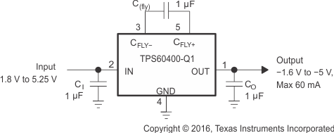
Only three external 1-μF capacitors are required to build a complete DC-DC charge pump inverter. Assembled in a 5-pin SOT-23 package, the complete converter can be built on a 50-mm2 board area. Replacing the Schottky diode typically needed for start-up into load with integrated circuitry can achieve additional board area and component count reduction.
The TPS6040x-Q1 can deliver a maximum output current of 60 mA, with a typical conversion efficiency of greater than 90% over a wide output current range. Three device options TPS60401/2/3-Q1 with 20-kHz, 50-kHz, and 250-kHz fixed frequency operation are available. TPS60400-Q1 device comes with a variable switching frequency to reduce operating current in applications with a wide load range and enables the design with low-value capacitors.
Device Information(1)
| PART NUMBER | PACKAGE | BODY SIZE (NOM) |
|---|---|---|
| TPS6040x-Q1 | SOT-23 (5) | 2.80 mm × 2.90 mm |
- For all available packages, see the orderable addendum at the end of the data sheet.
Typical Application Circuit

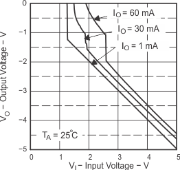
Output Voltage vs Input Voltage
