SLVSCQ7 April   2015 TPS61046

PRODUCTION DATA.  

  1. Features
  2. Applications
  3. Description
  4. Simplified Schematic
  5. Revision History
  6. Pin Configuration and Functions
  7. Specifications
    1. 7.1 Absolute Maximum Ratings
    2. 7.2 ESD Ratings
    3. 7.3 Recommended Operating Conditions
    4. 7.4 Thermal Information
    5. 7.5 Electrical Characteristics
    6. 7.6 Typical Characteristics
  8. Detailed Description
    1. 8.1 Overview
    2. 8.2 Functional Block Diagram
    3. 8.3 Feature Description
      1. 8.3.1 Under-Voltage Lockout
      2. 8.3.2 Enable and Disable
      3. 8.3.3 Soft Start
      4. 8.3.4 Over-voltage Protection
      5. 8.3.5 Output Short Circuit Protection
      6. 8.3.6 Thermal Shutdown
      7. 8.3.7 Device Functional Modes
        1. 8.3.7.1 PWM Mode
      8. 8.3.8 Power Save Mode
  9. Application and Implementation
    1. 9.1 Application Information
    2. 9.2 Typical Application - 12-V Output Boost Converter
      1. 9.2.1 Design Requirements
      2. 9.2.2 Detailed Design Procedure
        1. 9.2.2.1 Programming the Output Voltage
        2. 9.2.2.2 Inductor Selection
        3. 9.2.2.3 Input and Output Capacitor Selection
      3. 9.2.3 Application Performance Curves
    3. 9.3 System Examples
      1. 9.3.1 Fixed 12-V Output Voltage with Three External Components
  10. 10Power Supply Recommendations
  11. 11Layout
    1. 11.1 Layout Guidelines
    2. 11.2 Layout Example
  12. 12Device and Documentation Support
    1. 12.1 Device Support
      1. 12.1.1 Third-Party Products Disclaimer
    2. 12.2 Community Resources
    3. 12.3 Trademarks
    4. 12.4 Electrostatic Discharge Caution
    5. 12.5 Glossary
  13. 13Mechanical, Packaging, and Orderable Information

パッケージ・オプション

メカニカル・データ(パッケージ|ピン)
サーマルパッド・メカニカル・データ
発注情報

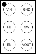
6 Pin Configuration and Functions

YFF Package
6-Ball WCSP
(Top View)
TPS61046 PO_slvscq7.gif

Pin Functions

PIN I/O DESCRIPTION
NAME NUMBER
EN C1 I Enable logic input. Logic high voltage enables the device. Logic low voltage disables the device and turns it into shutdown mode.
FB B1 I Voltage feedback of adjustable output voltage. Connect to the center tap of a resistor divider to program the output voltage. When it is connected to the VIN pin, the output voltage is set to 12 V by an internal feedback.
GND A2 PWR Ground
SW B2 PWR The switch pin of the converter. It is connected to the drain of the internal power MOSFET.
VIN A1 I IC power supply input
VOUT C2 PWR Output of the boost converter