SLVS776B January 2009 – November 2014 TPS61220 , TPS61221 , TPS61222
PRODUCTION DATA.
- 1 Features
- 2 Applications
- 3 Description
- 4 Simplified Schematic
- 5 Revision History
- 6 Pin Configuration and Functions
- 7 Specifications
- 8 Parameter Measurement Information
- 9 Detailed Description
- 10Applications and Implementation
- 11Power Supply Recommendations
- 12Layout
- 13Device and Documentation Support
- 14Mechanical, Packaging, and Orderable Information
9 Detailed Description
9.1 Overview
The TPS6122x is a high performance, high efficient family of switching boost converters. To achieve high efficiency, the power stage is realized as a synchronous-boost topology. For the power switching, two actively-controlled low-RDSon power MOSFETs are implemented.
9.2 Functional Block Diagrams
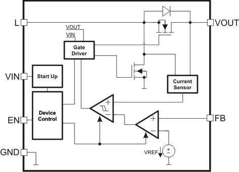 Figure 23. Functional Block Diagram (Adjustable Version)
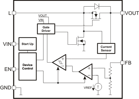 Figure 24. Functional Block Diagram (Fixed Output Voltage Version)
9.3 Feature Description
9.3.1 Controller Circuit
The device is controlled by a hysteretic current mode controller. This controller regulates the output voltage by keeping the inductor ripple current constant in the range of 200 mA and adjusting the offset of this inductor current depending on the output load. If the required average input current is lower than the average inductor current defined by this constant ripple current, the inductor current becomes discontinuous to keep the efficiency high under low-load conditions.
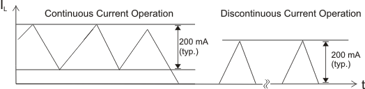 Figure 25. Hysteretic Current Operation
The output voltage VOUT is monitored via the feedback network which is connected to the voltage error amplifier. To regulate the output voltage, the voltage error amplifier compares this feedback voltage to the internal voltage reference and adjusts the required offset of the inductor current accordingly. In fixed output voltage devices, an internal feedback network is used to program the output voltage. In adjustable versions an external resistor divider is required.
The self-oscillating hysteretic current mode architecture is inherently stable and allows fast response to load variations. This architecture also allows using a wide range of inductor and capacitor values.
9.3.2 Device Enable And Shutdown Mode
The device is enabled when EN is driven high, and shut down when EN is low. During shutdown, the converter stops switching and all internal control circuitry is turned off. During shutdown, the input voltage is connected to the output through the back-gate diode of the rectifying MOSFET. This means that voltage is always present at the output, which can be as high as the input voltage or lower depending on the load.
9.3.3 Startup
After the EN pin is tied high, the device begins to operate. If the input voltage is not high enough to supply the control circuit properly, a startup oscillator operates the switches. During this phase, the switching frequency is controlled by the oscillator, and the maximum switch current is limited. When the device has built up the output voltage to approximately 1.8V, high enough to supply the control circuit, the device switches to its normal hysteretic current mode operation. The startup time depends on input voltage and load current.
9.3.4 Operation At Output Overload
If, in normal boost operation, the inductor current reaches the internal switch current limit threshold, the main switch is turned off to stop further increase of the input current. In this case the output voltage will decrease because the device cannot provide sufficient power to maintain the set output voltage.
If the output voltage drops below the input voltage, the backgate diode of the rectifying switch becomes forward biased, and current starts to flow through it. This diode cannot be turned off, so the current finally is only limited by the remaining DC resistances. As soon as the overload condition is removed, the converter resumes providing the set output voltage.
9.3.5 Undervoltage Lockout
An undervoltage lockout function stops the operation of the converter if the input voltage drops below the typical undervoltage lockout threshold. This function is implemented in order to prevent converter malfunction.
9.3.6 Overvoltage Protection
If, for any reason, the output voltage is not fed back properly to the input of the voltage amplifier, control of the output voltage is lost. Therefore an overvoltage protection is implemented to avoid the output voltage exceeding critical values for the device and possibly for the system it is supplying. For this protection, the TPS6122x output voltage is also monitored internally. If it reaches the internally programmed threshold of 6.5 V, typically the voltage amplifier regulates (limits) the output voltage to this value.
If the TPS6122x is used to drive LEDs, this feature protects the circuit if the LED fails.
9.3.7 Overtemperature Protection
The device has a built-in temperature sensor which monitors the internal IC junction temperature. If the temperature exceeds the programmed threshold (see electrical characteristics table), the device stops operating. As soon as the IC temperature has decreased below the programmed threshold, it starts operating again. To prevent unstable operation close to the region of overtemperature threshold, a built-in hysteresis is implemented.