JAJSFM1B June 2018 – January 2021 TPS61372
PRODUCTION DATA
- 1 特長
- 2 アプリケーション
- 3 概要
- 4 Revision History
- 5 Pin Configuration and Functions
- 6 Specifications
- 7 Detailed Description
-
8 Application and Implementation
- 8.1 Application Information
- 8.2
Typical Application
- 8.2.1 Design Requirements
- 8.2.2
Detailed Design Procedure
- 8.2.2.1 Custom Design With WEBENCH® Tools
- 8.2.2.2 Setting the Output Voltage
- 8.2.2.3 Selecting the Inductor
- 8.2.2.4 Selecting the Output Capacitors
- 8.2.2.5 Selecting the Input Capacitors
- 8.2.2.6 Loop Stability and Compensation
- 8.2.2.7 Loop Compensation Design Steps
- 8.2.2.8 Selecting the Bootstrap Capacitor
- 8.2.3 Application Curves
- 9 Power Supply Recommendations
- 10Layout
- 11Device and Documentation Support
- 12Mechanical, Packaging, and Orderable Information
パッケージ・オプション
デバイスごとのパッケージ図は、PDF版データシートをご参照ください。
メカニカル・データ(パッケージ|ピン)
- YKB|16
サーマルパッド・メカニカル・データ
発注情報
8.2.2.3 Selecting the Inductor
A boost converter normally requires two main passive components for storing the energy during power conversion: an inductor and an output capacitor. The inductor affects the steady state efficiency (including the ripple and efficiency) as well as the transient behavior and loop stability, which makes the inductor to be the most critical component in application.
When selecting the inductor, as well as the inductance, the other parameters of importance are:
- The maximum current rating (RMS and peak current should be considered)
- The series resistance
- Operating temperature
Choosing the inductor ripple current with the low ripple percentage of the average inductor current results in a larger inductance value, maximizes the potential output current of the converter, and minimizes EMI. The larger ripple results in a smaller inductance value and a physically smaller inductor, which improves transient response, but results in potentially higher EMI.
The rule of thumb in choosing the inductor is to make sure the inductor ripple current (ΔIL) is a certain percentage of the average current. The inductance can be calculated by Equation 2, Equation 3, and Equation 4:
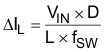
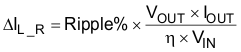
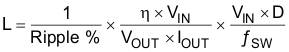
where
- ΔIL is the peak-peak inductor current ripple
- VIN is the input voltage
- D is the duty cycle
- L is the inductor
- ƒSW is the switching frequency
- Ripple% is the ripple ration versus the DC current
- VOUT is the output voltage
- IOUT is the output current
- η is the efficiency
The current flowing through the inductor is the inductor ripple current plus the average input current. During power up, load faults, or transient load conditions, the inductor current can increase above the peak inductor current calculated.
Inductor values can have ±20% or even ±30% tolerance with no current bias. When the inductor current approaches the saturation level, its inductance can decrease 20% to 35% from the value at 0-A bias current depending on how the inductor vendor defines saturation. When selecting an inductor, make sure its rated current, especially the saturation current, is larger than its peak current during the operation.
The inductor peak current varies as a function of the load, the switching frequency, and the input and output voltages and it can be calculated by Equation 5 and Equation 6.
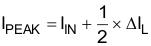
where
- IPEAK is the peak current of the inductor
- IIN is the input average current
- ΔIL is the ripple current of the inductor
The input DC current is determined by the output voltage, the output current, and efficiency can be calculated by:
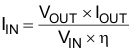
where
- IIN is the input current of the inductor
- VOUT is the output voltage
- VIN is the input voltage
- η is the efficiency
While the inductor ripple current depends on the inductance, the frequency, the input voltage, and duty cycle calculated by Equation 2, replace Equation 2, Equation 6 into Equation 5 to calculate the inductor peak current:
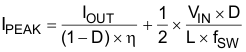
where
- IPEAK is the peak current of the inductor
- IOUT is the output current
- D is the duty cycle
- η is the efficiency
- VIN is the input voltage
- L is the inductor
- ƒSW is the switching frequency
The heat rating current (RMS) is calculated by Equation 8:
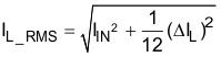
where
- IL_RMS is the RMS current of the inductor
- IIN is the input current of the inductor
- ΔIL is the ripple current of the inductor
It is important that the peak current does not exceed the inductor saturation current and the RMS current is not over the temperature related rating current of the inductors.
For a given physical inductor size, increasing inductance usually results in an inductor with lower saturation current. The total losses of the coil consists of the DC resistance ( DCR ) loss and the following frequency dependent loss:
- The losses in the core material (magnetic hysteresis loss, especially at high switching frequencies)
- Additional losses in the conductor from the skin effect (current displacement at high frequencies)
- Magnetic field losses of the neighboring windings (proximity effect)
For a certain inductor, the larger current ripple (smaller inductor) generates the higher DC and frequency-dependent loss. An inductor with lower DCR is basically recommended for higher efficiency. However, it is usually a tradeoff between the loss and footprint.
The following inductor series in Table 8-2 from the different suppliers are recommended.
| PART NUMBER | L (μH) | DCR Typ (mΩ) TYP. | SATURATION CURRENT / TYP. | SIZE (L × W × H mm) | VENDOR(1) |
|---|---|---|---|---|---|
| XAL4020-222ME | 2.2 | 35 | 5.6 | 4 x 4 x 2 | Coilcraft |
| DFE322512F-2R2M=P2 | 2.2 | 66 | 2.6 | 3.2 x 2.5 x 1.2 | Murata |
| DFE322520FD-4R7M# | 4.7 | 98 | 3.4 | 3.2 x 2.5 x 2.0 | Murata |