JAJSFM1B June 2018 – January 2021 TPS61372
PRODUCTION DATA
- 1 特長
- 2 アプリケーション
- 3 概要
- 4 Revision History
- 5 Pin Configuration and Functions
- 6 Specifications
- 7 Detailed Description
-
8 Application and Implementation
- 8.1 Application Information
- 8.2
Typical Application
- 8.2.1 Design Requirements
- 8.2.2
Detailed Design Procedure
- 8.2.2.1 Custom Design With WEBENCH® Tools
- 8.2.2.2 Setting the Output Voltage
- 8.2.2.3 Selecting the Inductor
- 8.2.2.4 Selecting the Output Capacitors
- 8.2.2.5 Selecting the Input Capacitors
- 8.2.2.6 Loop Stability and Compensation
- 8.2.2.7 Loop Compensation Design Steps
- 8.2.2.8 Selecting the Bootstrap Capacitor
- 8.2.3 Application Curves
- 9 Power Supply Recommendations
- 10Layout
- 11Device and Documentation Support
- 12Mechanical, Packaging, and Orderable Information
パッケージ・オプション
デバイスごとのパッケージ図は、PDF版データシートをご参照ください。
メカニカル・データ(パッケージ|ピン)
- YKB|16
サーマルパッド・メカニカル・データ
発注情報
8.2.2.4 Selecting the Output Capacitors
The output capacitor is mainly selected to meet the requirements at load transient or steady state. Then the loop is compensated for the output capacitor selected. The output ripple voltage is related to the equivalent series resistance (ESR) of the capacitor and its capacitance. Assuming a capacitor with zero ESR, the minimum capacitance needed for a given ripple can be calculated by Equation 9:
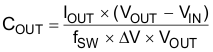
where
- COUT is the output capacitor
- IOUT is the output current
- VOUT is the output voltage
- VIN is the input voltage
- ΔV is the output voltage ripple required
- ƒSW is the switching frequency
The additional output ripple component caused by ESR is calculated by Equation 10:
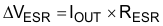
where
- ΔVESR is the output voltage ripple caused by ESR
- RESR is the resistor in series with the output capacitor
For the ceramic capacitor, the ESR ripple can be neglected. However, for the tantalum or electrolytic capacitors, it must be considered if used.
Care must be taken when evaluating the rating of a ceramic capacitor under the DC bias. Ceramic capacitors can derate by as much as 70% of its capacitance at its rated voltage. Therefore, enough margins on the voltage rating should be considered to ensure adequate capacitance at the required output voltage.
| PART NUMBER | C (μF) | PIECES | DESCRIPTION | SIZE | VENDOR(1) |
|---|---|---|---|---|---|
| GRM188R61E106MA73D | 10 | 3 | X5R, 0603, 5 V, ±20% tolerance | 0603 | Murata |