JAJSBM1E November   2011  – October 2021 TPS62150 , TPS62150A , TPS62151 , TPS62152 , TPS62153

PRODUCTION DATA  

  1. 特長
  2. アプリケーション
  3. 概要
  4. Revision History
  5. Device Comparison Table
  6. Pin Configuration and Functions
  7. Specifications
    1. 7.1 Absolute Maximum Ratings (1)
    2. 7.2 ESD Ratings
    3. 7.3 Recommended Operating Conditions
    4. 7.4 Thermal Information
    5. 7.5 Electrical Characteristics
    6. 7.6 Typical Characteristics
  8. Detailed Description
    1. 8.1 Overview
    2. 8.2 Functional Block Diagrams
    3. 8.3 Feature Description
      1. 8.3.1 Enable / Shutdown (EN)
      2. 8.3.2 Soft Start or Tracking (SS/TR)
      3. 8.3.3 Power Good (PG)
      4. 8.3.4 Pin-Selectable Output Voltage (DEF)
      5. 8.3.5 Frequency Selection (FSW)
      6. 8.3.6 Undervoltage Lockout (UVLO)
      7. 8.3.7 Thermal Shutdown
    4. 8.4 Device Functional Modes
      1. 8.4.1 Pulse-Width Modulation (PWM) Operation
      2. 8.4.2 Power-Save Mode Operation
      3. 8.4.3 100% Duty-Cycle Operation
      4. 8.4.4 Current-Limit and Short-Circuit Protection
  9. Application and Implementation
    1. 9.1 Application Information
    2. 9.2 Typical Application
      1. 9.2.1 Design Requirements
      2. 9.2.2 Detailed Design Procedure
        1. 9.2.2.1 Programming the Output Voltage
        2. 9.2.2.2 External Component Selection
          1. 9.2.2.2.1 Inductor Selection
          2. 9.2.2.2.2 Capacitor Selection
            1. 9.2.2.2.2.1 Output Capacitor
            2. 9.2.2.2.2.2 Input Capacitor
            3. 9.2.2.2.2.3 Soft-Start Capacitor
        3. 9.2.2.3 Tracking Function
        4. 9.2.2.4 Output Filter and Loop Stability
      3. 9.2.3 Application Curves
    3. 9.3 System Examples
      1. 9.3.1 LED Power Supply
      2. 9.3.2 Active Output Discharge
      3. 9.3.3 Inverting Power Supply
      4. 9.3.4 Various Output Voltages
  10. 10Power Supply Recommendations
  11. 11Layout
    1. 11.1 Layout Guidelines
    2. 11.2 Layout Example
      1. 11.2.1 Thermal Considerations
  12. 12Device and Documentation Support
    1. 12.1 Device Support
      1. 12.1.1 Third-Party Products Disclaimer
    2. 12.2 Documentation Support
      1. 12.2.1 Related Documentation
    3. 12.3 Receiving Notification of Documentation Updates
    4. 12.4 サポート・リソース
    5. 12.5 Trademarks
    6. 12.6 Electrostatic Discharge Caution
    7. 12.7 Glossary
  13. 13Mechanical, Packaging, and Orderable Information

パッケージ・オプション

メカニカル・データ(パッケージ|ピン)
サーマルパッド・メカニカル・データ
発注情報
Soft-Start Capacitor

A capacitance connected between the SS/TR pin and AGND allows a user-programmable start-up slope of the output voltage. A constant-current source supplies 2.5 µA to charge the external capacitance. The capacitor required for a given soft-start ramp time for the output voltage is given by:
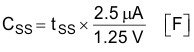
Equation 10. GUID-0267F72E-7E82-465E-9DA8-37042EBA8DD4-low.gif

where

  • CSS is the capacitance (F) required at the SS/TR pin
  • tSS is the desired soft-start ramp time (s)
Note:

DC bias effect: High capacitance ceramic capacitors have a DC bias effect, which has a strong influence on the final effective capacitnace. Therefore, selecting the right capacitor value requires careful choice. Package size and voltage rating in combination with delectric material are responsible for differences betweeen the rated capacitor value and the effective capacitance.