JAJSJL4B August 2020 – March 2021 TPS62912 , TPS62913
PRODUCTION DATA
- 1 特長
- 2 アプリケーション
- 3 概要
- 4 Revision History
- 5 Pin Configuration and Functions
- 6 Specifications
-
7 Detailed Description
- 7.1 Overview
- 7.2 Functional Block Diagram
- 7.3
Feature Description
- 7.3.1 Smart Config (S-CONF)
- 7.3.2 Device Enable (EN/SYNC)
- 7.3.3 Device Synchronization (EN/SYNC)
- 7.3.4 Spread Spectrum Modulation
- 7.3.5 Output Discharge
- 7.3.6 Undervoltage Lockout (UVLO)
- 7.3.7 Power-Good Output
- 7.3.8 Noise Reduction and Soft-Start Capacitor (NR/SS)
- 7.3.9 Current Limit and Short Circuit Protection
- 7.3.10 Thermal Shutdown
- 7.4 Device Functional Modes
- 8 Application and Implementation
- 9 Power Supply Recommendations
- 10Layout
- 11Device and Documentation Support
- 12Mechanical, Packaging, and Orderable Information
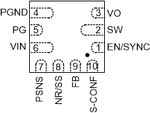
5 Pin Configuration and Functions
 Figure 5-1 10-Pin QFN RPU Package (Top
View)
Figure 5-1 10-Pin QFN RPU Package (Top
View)Table 5-1 Pin Functions
| PIN | I/O | DESCRIPTION | |
|---|---|---|---|
| NO. | NAME | ||
| 1 | EN/SYNC | I | Enable/Disable pin including threshold-comparator. Connect to logic low to disable the device. Pull high to enable the device. This pin has an internal pulldown resistor of typically 500 kΩ when the device is disabled. Apply a clock to this pin to synchronize the device. |
| 2 | SW | I/O | Switch pin of the power stage |
| 3 | VO | I | Output voltage sense pin. This pin needs to be connected directly after the first inductor. |
| 4 | PGND | Power ground connection | |
| 5 | PG | O | Open-drain power-good output. This pin is pulled to GND when VOUT is below the power-good threshold. It requires a pullup resistor to output a logic high. It can be left open or tied to GND if not used. |
| 6 | VIN | I | Power supply input voltage pin |
| 7 | PSNS | I | Power sense ground. Connect directly to the ground plane. |
| 8 | NR/SS | O | A capacitor connected to this pin sets the soft-start time and low frequency noise level of the device. |
| 9 | FB | I | Feedback pin of the device |
| 10 | S-CONF | O | Smart Configuration pin. This pin configures the operation modes of the device. See Table 7-1. |