JAJSJL4B August 2020 – March 2021 TPS62912 , TPS62913
PRODUCTION DATA
- 1 特長
- 2 アプリケーション
- 3 概要
- 4 Revision History
- 5 Pin Configuration and Functions
- 6 Specifications
-
7 Detailed Description
- 7.1 Overview
- 7.2 Functional Block Diagram
- 7.3
Feature Description
- 7.3.1 Smart Config (S-CONF)
- 7.3.2 Device Enable (EN/SYNC)
- 7.3.3 Device Synchronization (EN/SYNC)
- 7.3.4 Spread Spectrum Modulation
- 7.3.5 Output Discharge
- 7.3.6 Undervoltage Lockout (UVLO)
- 7.3.7 Power-Good Output
- 7.3.8 Noise Reduction and Soft-Start Capacitor (NR/SS)
- 7.3.9 Current Limit and Short Circuit Protection
- 7.3.10 Thermal Shutdown
- 7.4 Device Functional Modes
- 8 Application and Implementation
- 9 Power Supply Recommendations
- 10Layout
- 11Device and Documentation Support
- 12Mechanical, Packaging, and Orderable Information
8.2.2.2.1 Switching Frequency Selection
The switching frequency can be chosen to optimize efficiency (1 MHz) or ripple/noise (2.2 MHz). Using the 2.2-MHz setting increases the gain of the feedback loop and can result in lower output noise. However, additional considerations for minimum on-time and duty cycle must also be considered. First, calculate the duty cycle using Equation 3. Higher efficiency results in a shorter on-time, so a conservative approach is to use a higher efficiency than expected in the application.

where
- η is the estimated efficiency (use the value from the efficiency curves or 0.9 as an conservative assumption)
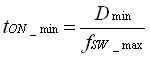
Then, calculate the on-time with both 1 MHz and 2.2 MHz using Equation 4. The on-time must always remain above the minimum on-time of 70 nsec. Use the maximum input voltage and maximum efficiency to determine the minimum duty cycle, Dmin. Use the maximum switching frequency for fSW.
then
-
If tON_min min < 70 ns with 2.2 MHz, use 1 MHz.
-
If tON_min min < 70 ns with 1 MHz, reduce the maximum input voltage.
-
If tON_min min ≥ 70 ns for both cases, use 1 MHz for highest efficiency, or 2.2 MHz for lowest noise and ripple.