JAJSJL4B August 2020 – March 2021 TPS62912 , TPS62913
PRODUCTION DATA
- 1 特長
- 2 アプリケーション
- 3 概要
- 4 Revision History
- 5 Pin Configuration and Functions
- 6 Specifications
-
7 Detailed Description
- 7.1 Overview
- 7.2 Functional Block Diagram
- 7.3
Feature Description
- 7.3.1 Smart Config (S-CONF)
- 7.3.2 Device Enable (EN/SYNC)
- 7.3.3 Device Synchronization (EN/SYNC)
- 7.3.4 Spread Spectrum Modulation
- 7.3.5 Output Discharge
- 7.3.6 Undervoltage Lockout (UVLO)
- 7.3.7 Power-Good Output
- 7.3.8 Noise Reduction and Soft-Start Capacitor (NR/SS)
- 7.3.9 Current Limit and Short Circuit Protection
- 7.3.10 Thermal Shutdown
- 7.4 Device Functional Modes
- 8 Application and Implementation
- 9 Power Supply Recommendations
- 10Layout
- 11Device and Documentation Support
- 12Mechanical, Packaging, and Orderable Information
10.2 Layout Example
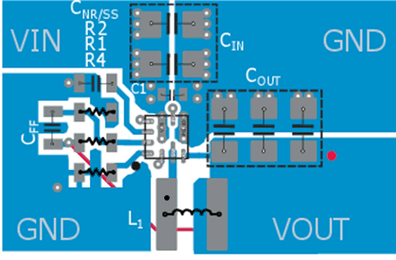
 Figure 10-1 Recommended
Layout for Single L-C Filter
Figure 10-1 Recommended
Layout for Single L-C FilterNote: The start winding of
the inductor, as shown in the figures as a black dot, needs to be
connected to the DC/DC converter switch pin, SW, to minimize
capacitive coupling to the surrounding area.
Note: The red dot indicates where the feedback sense should be placed for
the best DC regulation. For a single L-C configuration, it is
placed near the VOUT capacitors. For a second L-C filter design,
the feedback sense is placed near the load after the VOUT_FILT
capacitors.
 Figure 10-2 Recommended
Layout for Design with Second L-C Filter
Figure 10-2 Recommended
Layout for Design with Second L-C FilterNote: The ferrite bead can be placed closer to the device as long as it is
outside the keep out area, as shown in the figure as a red
rectangular area. This placement avoids capacitive and
electromagnetic coupling to the output of the ferrite bead. If the
ferrite bead is placed in the keep out area, the filtering effect of
the ferrite bead is greatly reduced. If the ferrite bead is routed
through a via to the back side of the board, ensure adequate ground
plane between the layers if the ferrite bead will be in this area.