JAJSHU4B August 2012 – August 2019 TPS63036
PRODUCTION DATA.
- 1 特長
- 2 アプリケーション
- 3 概要
- 4 改訂履歴
- 5 Pin Configuration and Functions
- 6 Specifications
- 7 Detailed Description
- 8 Application and Implementation
- 9 Power Supply Recommendations
- 10Layout
- 11デバイスおよびドキュメントのサポート
- 12メカニカル、パッケージ、および注文情報
7.4.3 Control Loop
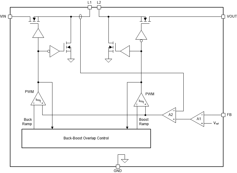
The average inductor current is regulated by a fast current regulator loop which is controlled by a voltage control loop. Figure 3 shows the control loop.
The noninverting input of the trans-conductance amplifier Gmv can be assumed to be constant. The output of Gmv defines the average inductor current. The inductor current is reconstructed measuring the current through the high-side buck MOSFET. This current corresponds exactly to the inductor current in boost mode. In buck mode the current is measured during the ON-time of the same MOSFET. During the OFF-time the current is reconstructed internally starting from the peak value reached at the end of the ON-time cycle. The average current is then compared to the desired value and the difference, or current error, is amplified and compared to the sawtooth ramp of either the buck or the boost.
The Buck-Boost Overlap Control makes sure that the classical buck-boost function, which would cause two switches to be on every half a cycle, is avoided. Thanks to this block whenever all switches becomes active during one clock cycle, the two ramps are shifted away from each other, on the other hand when there is no switching activities because there is a gap between the ramps, the ramps are moved closer together. As a result the number of classical buck-boost cycles or no switching is reduced to a minimum and high-efficiency values have been achieved.
Slope compensation is not required to avoid subharmonic oscillation which are otherwise observed when working with peak current mode control with D > 0.5.
Nevertheless the amplified inductor current downslope at one input of the PWM comparator must not exceed the oscillator ramp slope at the other comparator input. This purpose is reached limiting the gain of the current amplifier.
 Figure 3. Average Current Mode Control