JAJSIY9D March 2020 – October 2020 TPS63900
PRODUCTION DATA
- 1 特長
- 2 アプリケーション
- 3 概要
- 4 Revision History
- 5 Pin Configuration and Functions
- 6 Specifications
-
7 Detailed Description
- 7.1 Overview
- 7.2 Functional Block Diagram
- 7.3 Feature Description
- 7.4 Device Functional Modes
- 8 Application and Implementation
- 9 Power Supply Recommendations
- 10Layout
- 11Device and Documentation Support
- 12Mechanical, Packaging, and Orderable Information
パッケージ・オプション
メカニカル・データ(パッケージ|ピン)
- DSK|10
サーマルパッド・メカニカル・データ
- DSK|10
発注情報
7.3.1 Trapezoidal Current Control
Figure 7-1 shows a simplified block diagram of the power stage of the device. Inductor current is sensed in series with Q1 (the peak current) and Q4 (the valley current).
 Figure 7-1 Power Stage Simplified Block Diagram
The device uses a trapezoidal inductor current to regulate its output under all operating conditions. Thus, the device only has one operating mode and does not display any of the mode-change transients or unpredictable switching displayed by many other buck-boost devices.
There are four phases of operation:
- Phase A – Q1 and Q3 are on and Q2 and Q4 are off
- Phase B – Q1 and Q4 are on and Q2 and Q3 are off
- Phase C – Q2 and Q4 are on and Q1 and Q3 are off
- Phase D – Q2 and Q3 are on and Q1 and Q4 are off
Figure 7-2 shows the inductor current waveform when VI > VO, Figure 7-3 shows the current waveform when VI = VO, and Figure 7-4 shows the current waveform when VI < VO.
Figure 7-2 through Figure 7-4 show the typical waveforms during continuous conduction mode (CCM) switching for three operating conditions. During discontinuous conduction mode (DCM), the typical inductor current waveforms look similar to CCM with Phase D at 0 A inductor current. In deep boost mode, where VI << VO, Phase C length gradually decreases to zero until the switching waveform becomes triangular.
") Figure 7-2 Inductor Current Waveform when VI > VO (CCM)
Figure 7-2 Inductor Current Waveform when VI > VO (CCM)") Figure 7-3 Inductor Current Waveform when VI = VO (CCM)
Figure 7-3 Inductor Current Waveform when VI = VO (CCM)") Figure 7-4 Inductor Current Waveform when VI < VO (CCM)
Figure 7-4 Inductor Current Waveform when VI < VO (CCM)The ideal relationship between VI and VO (that is, assuming no losses) is
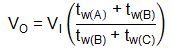
where
- VI is the input voltage
- VO is the output voltage
- tw(A) is the duration of phase A
- tw(B) is the duration of phase B
- tw(C) is the duration of phase C
By varying relative duration of each phase, the device can regulate VO to be less than, equal to, or greater than VI.