JAJSGJ5E November 2014 – February 2021 TPS65218
PRODUCTION DATA
- 1 特長
- 2 アプリケーション
- 3 概要
- 4 Revision History
- 5 Pin Configuration and Functions
- 6 Specifications
-
7 Detailed Description
- 7.1 Overview
- 7.2 Functional Block Diagram
- 7.3
Feature Description
- 7.3.1
Wake-Up and Power-Up and Power-Down Sequencing
- 7.3.1.1 Power-Up Sequencing
- 7.3.1.2 Power-Down Sequencing
- 7.3.1.3 Strobe 1 and Strobe 2
- 7.3.1.4 Supply Voltage Supervisor and Power-Good (PGOOD)
- 7.3.1.5 Backup Supply Power-Good (PGOOD_BU)
- 7.3.1.6 Internal LDO (INT_LDO)
- 7.3.1.7 Current Limited Load Switches
- 7.3.1.8 LDO1
- 7.3.1.9 Coin Cell Battery Voltage Acquisition
- 7.3.1.10 UVLO
- 7.3.1.11 Power-Fail Comparator
- 7.3.1.12 Battery-Backup Supply Power-Path
- 7.3.1.13 DCDC3 and DCDC4 Power-Up Default Selection
- 7.3.1.14 I/O Configuration
- 7.3.1.15 Push Button Input (PB)
- 7.3.1.16 AC_DET Input (AC_DET)
- 7.3.1.17 Interrupt Pin (INT)
- 7.3.1.18 I2C Bus Operation
- 7.3.1
Wake-Up and Power-Up and Power-Down Sequencing
- 7.4 Device Functional Modes
- 7.5 Register Maps
- 8 Application and Implementation
- 9 Power Supply Recommendations
- 10Layout
- 11Device and Documentation Support
- 12Mechanical, Packaging, and Orderable Information
パッケージ・オプション
メカニカル・データ(パッケージ|ピン)
サーマルパッド・メカニカル・データ
発注情報
7.3.1.18 I2C Bus Operation
The TPS65218 hosts a slave I2C interface (address 0x24) that supports data rates up to 400 kbps, auto-increment addressing. (1)
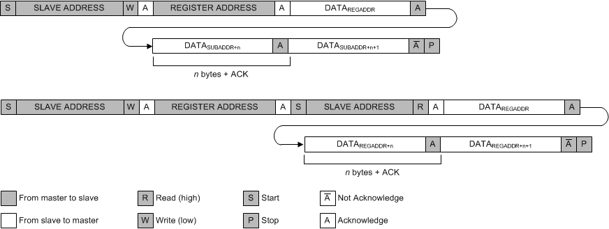
 Figure 7-30 Subaddress in I2C Transmission
The I2C bus is a communications link between a controller and a series of slave terminals. The link is established using a two-wired bus consisting of a serial clock signal (SCL) and a serial data signal (SDA). The serial clock is sourced from the controller in all cases where the serial data line is bi-directional for data communication between the controller and the slave terminals. Each device has an open drain output to transmit data on the serial data line. An external pullup resistor must be placed on the serial data line to pull the drain output high during data transmission.
Data transmission initiates with a start bit from the controller as shown in Figure 7-32. The start condition is recognized when the SDA line transitions from high to low during the high portion of the SCL signal. Upon reception of a start bit, the device receives serial data on the SDA input and checks for valid address and control information. If the appropriate slave address is set for the device, the device issues an acknowledge pulse and prepares to receive register address and data. Data transmission is completed by either the reception of a stop condition or the reception of the data word sent to the device. A stop condition is recognized as a low to high transition of the SDA input during the high portion of the SCL signal. All other transitions of the SDA line must occur during the low portion of the SCL signal. An acknowledge issues after the reception of valid slave address, register-address, and data words. The I2C interfaces an auto-sequence through the register addresses, so that multiple data words can be sent for a given I2C transmission. Reference Figure 7-31 and Figure 7-32 for details.

 Figure 7-32 I2C Protocol and Transmission Timing I2C Start Stop and Acknowledge Protocol
 Figure 7-33 I2C Protocol and Transmission Timing I2C Data Transmission Timing