JAJSEF6L August 2013 – February 2019 TPS659038-Q1 , TPS659039-Q1
PRODUCTION DATA.
- 1 デバイスの概要
- 2 改訂履歴
- 3 Device Comparison
- 4 Pin Configuration and Functions
-
5 Specifications
- 5.1 Absolute Maximum Ratings
- 5.2 ESD Ratings
- 5.3 Recommended Operating Conditions
- 5.4 Thermal Information
- 5.5 Electrical Characteristics: Latch Up Rating
- 5.6 Electrical Characteristics: LDO Regulator
- 5.7 Electrical Characteristics: Dual-Phase (SMPS12 and SMPS45) and Triple-Phase (SMPS123 and SMPS457) Regulators
- 5.8 Electrical Characteristics: Stand-Alone Regulators (SMPS3, SMPS6, SMPS7, SMPS8, and SMPS9)
- 5.9 Electrical Characteristics: Reference Generator (Bandgap)
- 5.10 Electrical Characteristics: 16-MHz Crystal Oscillator, 32-kHz RC Oscillator, and Output Buffers
- 5.11 Electrical Characteristics: DC-DC Clock Sync
- 5.12 Electrical Characteristics: 12-Bit Sigma-Delta ADC
- 5.13 Electrical Characteristics: Thermal Monitoring and Shutdown
- 5.14 Electrical Characteristics: System Control Thresholds
- 5.15 Electrical Characteristics: Current Consumption
- 5.16 Electrical Characteristics: Digital Input Signal Parameters
- 5.17 Electrical Characteristics: Digital Output Signal Parameters
- 5.18 Electrical Characteristics: I/O Pullup and Pulldown Resistance
- 5.19 I2C Interface Timing Requirements
- 5.20 SPI Timing Requirements
- 5.21 Typical Characteristics
-
6 Detailed Description
- 6.1 Overview
- 6.2 Functional Block Diagrams
- 6.3
Feature Description
- 6.3.1 Power Management
- 6.3.2
Power Resources (Step-Down and Step-Up SMPS Regulators, LDOs)
- 6.3.2.1
Step-Down Regulators
- 6.3.2.1.1 Sync Clock Functionality
- 6.3.2.1.2 Output Voltage and Mode Selection
- 6.3.2.1.3 Current Monitoring and Short Circuit Detection
- 6.3.2.1.4 POWERGOOD
- 6.3.2.1.5 DVS-Capable Regulators
- 6.3.2.1.6 Non DVS-Capable Regulators
- 6.3.2.1.7 Step-Down Converters SMPS12 and SMPS123
- 6.3.2.1.8 Step-Down Converter SMPS45 and SMPS457
- 6.3.2.1.9 Step-Down Converters SMPS3, SMPS6, SMPS7, SMPS8, and SMPS9
- 6.3.2.2 LDOs – Low Dropout Regulators
- 6.3.2.1
Step-Down Regulators
- 6.3.3 Long-Press Key Detection
- 6.3.4 RTC
- 6.3.5 GPADC – 12-Bit Sigma-Delta ADC
- 6.3.6 General-Purpose I/Os (GPIO Terminals)
- 6.3.7 Thermal Monitoring
- 6.3.8 Interrupts
- 6.3.9 Control Interfaces
- 6.3.10 Device Identification
- 6.4 Device Functional Modes
-
7 Application and Implementation
- 7.1 Application Information
- 7.2
Typical Application
- 7.2.1 Design Requirements
- 7.2.2 Detailed Design Procedure
- 7.2.3 Application Curves
- 8 Power Supply Recommendations
- 9 Layout
- 10デバイスおよびドキュメントのサポート
- 11メカニカル、パッケージ、および注文情報
パッケージ・オプション
デバイスごとのパッケージ図は、PDF版データシートをご参照ください。
メカニカル・データ(パッケージ|ピン)
- ZWS|169
サーマルパッド・メカニカル・データ
発注情報
6.4.10 Watchdog Timer (WDT)
The watchdog timer has two modes of operation, periodic mode and interrupt mode.
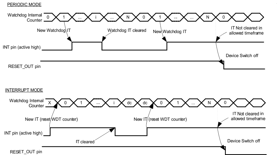
In periodic mode, an interrupt is generated with a regular period N that is defined by the WATCHDOG.TIMER setting. This interrupt is generated at the beginning of the period (when the watchdog internal counter equals 1). The IC initiates a shutdown at the end of the period (when the internal counter has reached N) only if the interrupt has not been cleared within the defined time frame (0 to N). In this mode, when the interrupt is cleared, the internal counter is not reset. The counter continues to count until it reaches the maximum value (defined by the TIMER setting) and automatically rolls over to 0 in order to start a new counting period. Regardless of when the interrupt is cleared within a given period (N), the next interrupt is generated only when the ongoing period completes (reaches N). The internal watchdog counter is initialized and kept at 0 as long as the RESET_OUT terminal is low. The counter begins counting as soon as the RESET_OUT terminal is released.
In interrupt mode, any interrupt source resets the watchdog counter and begins the counting. If the sources of the interrupts are not cleared (INT line released) before the end of the predefined period N (set by WATCHDOG.TIMER setting) then the IC initiates a shutdown. If the sources of the interrupts are cleared within the predefined period, then the watchdog counter is discarded (DC) and no shutdown sequence is initiated.
By default, the watchdog is disabled.
Figure 6-26 shows the watchdog timings.
 Figure 6-26 Watchdog Timing Diagrams