JAJSMN7C september 2021 – june 2023 TPS7A94
PRODUCTION DATA
- 1
- 1 特長
- 2 アプリケーション
- 3 概要
- 4 Revision History
- 5 Pin Configuration and Functions
- 6 Specifications
-
7 Detailed Description
- 7.1 Overview
- 7.2 Functional Block Diagram
- 7.3
Feature Description
- 7.3.1 Output Voltage Setting and Regulation
- 7.3.2 Ultra-Low Noise and Ultra-High Power-Supply Rejection Ratio (PSRR)
- 7.3.3 Programmable Current Limit and Power-Good Threshold
- 7.3.4 Programmable Soft Start (NR/SS Pin)
- 7.3.5 Precision Enable and UVLO
- 7.3.6 Active Discharge
- 7.3.7 Thermal Shutdown Protection (TSD)
- 7.4 Device Functional Modes
-
8 Application and Implementation
- 8.1
Application Information
- 8.1.1 Output Voltage Restart (Overshoot Prevention Circuit)
- 8.1.2 Precision Enable (External UVLO)
- 8.1.3 Undervoltage Lockout (UVLO) Operation
- 8.1.4 Dropout Voltage (VDO)
- 8.1.5 Power-Good Feedback (FB_PG Pin) and Power-Good Threshold (PG Pin)
- 8.1.6 Adjusting the Factory-Programmed Current Limit
- 8.1.7 Programmable Soft-Start and Noise-Reduction (NR/SS Pin)
- 8.1.8 Inrush Current
- 8.1.9 Optimizing Noise and PSRR
- 8.1.10 Adjustable Operation
- 8.1.11 Paralleling for Higher Output Current and Lower Noise
- 8.1.12 Recommended Capacitor Types
- 8.1.13 Load Transient Response
- 8.1.14 Power Dissipation (PD)
- 8.1.15 Estimating Junction Temperature
- 8.1.16 TPS7A94EVM-046 Thermal Analysis
- 8.2 Typical Application
- 8.3 Power Supply Recommendations
- 8.4 Layout
- 8.1
Application Information
- 9 Device and Documentation Support
- 10Mechanical, Packaging, and Orderable Information
パッケージ・オプション
デバイスごとのパッケージ図は、PDF版データシートをご参照ください。
メカニカル・データ(パッケージ|ピン)
- DSC|10
サーマルパッド・メカニカル・データ
発注情報
8.1.13 Load Transient Response
For best transient response, use the nominal value or larger capacitor from OUT to ground as listed in the Recommended Operating ConditionsRecommended Operating Conditions table. Place the output capacitor as close to the OUT and GND pins of the device as possible.
For best transient response and to minimize input impedance, use the nominal value or larger capacitor from IN to ground as listed in the Recommended Operating ConditionsRecommended Operating Conditions table. Place the input capacitor as close to the IN and GND pins of the device as possible.
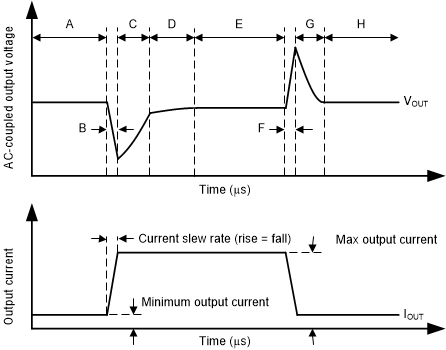
The load-step transient response is the LDO output voltage response to load current changes. There are two key transitions during a load transient response: the transition from a light to a heavy load, and the transition from a heavy to a light load. The regions shown in Figure 8-18 are broken down in this section. Regions A, E, and H are where the output voltage is in steady-state regulation.
 Figure 8-18 Load Transient
Waveform
Figure 8-18 Load Transient
WaveformDuring transitions from a light load to a heavy load:
- The initial voltage dip is a result of the depletion of the output capacitor charge and parasitic impedance to the output capacitor (region B)
- Recovery from the dip results from the LDO increasing the sourcing current, and leads to output voltage regulation (region C)
During transitions from a heavy load to a light load:
- The initial voltage rise results from the LDO sourcing a large current, and leads to the output capacitor charge to increase (region F)
- Recovery from the rise results from the LDO decreasing the sourcing current in combination with the load discharging the output capacitor (region G)
Transitions between current levels changes the internal power dissipation because the device is a high-current device (region D). The change in power dissipation changes the die temperature during these transitions, and leads to a slightly different voltage level. This temperature-dependent output voltage level shows up in the various load transient responses.
A larger output capacitance reduces the peaks during a load transient but slows down the response time of the device. A larger dc load also reduces the peaks because the amplitude of the transition is lowered and a higher current discharge path is provided for the output capacitor.