JAJSGH9F February 2016 – January 2023 TPS82130
PRODUCTION DATA
- 1 特長
- 2 アプリケーション
- 3 概要
- 4 Revision History
- 5 Pin Configuration and Functions
- 6 Specifications
- 7 Detailed Description
- 8 Application and Implementation
- 9 Device and Documentation Support
- 10Mechanical, Packaging, and Orderable Information
7.3.1 PWM and PSM Operation
The TPS82130 includes an on-time (tON) circuitry. tON, in steady-state operation in PWM and PSM modes, is estimated as:
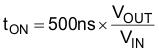
In PWM mode, the TPS82130 operates with pulse width modulation in continuous conduction mode (CCM) with a tON shown in Equation 1 at medium and heavy load currents. A PWM switching frequency of typically 2.0 MHz is achieved by this tON circuitry. The device operates in PWM mode as long as the output current is higher than half of the ripple current of the inductor estimated by Equation 2.
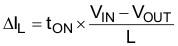
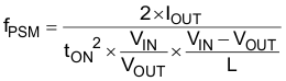
To maintain high efficiency at light loads, the device enters power save mode seamlessly when the load current decreases. This happens when the load current becomes smaller than half of the ripple current of the inductor. In PSM, the converter operates with reduced switching frequency and with a minimum quiescent current to maintain high efficiency. PSM is also based on the tON circuitry. The switching frequency in PSM is estimated as:
In PSM, the output voltage rises slightly above the nominal output voltage in PWM mode. This effect is reduced by increasing the output capacitance. The output voltage accuracy in PSM operation is reflected in GUID-E8F946A2-8401-42B5-B3A9-BA8823242976.html#GUID-E8F946A2-8401-42B5-B3A9-BA8823242976 and given for a 22-µF output capacitor.
For very small output voltages, an absolute minimum on time of approximately 80 ns is kept to limit switching losses. The operating frequency is thereby reduced from its nominal value, which keeps efficiency high. Also, the off time can reach its minimum value at high duty cycles. The output voltage remains regulated in such cases.
When VIN decreases to typically 15% above VOUT, the TPS82130 cannot enter power save mode, regardless of the load current. The device maintains output regulation in PWM mode.