JAJSD93 June   2017 TPS82150

PRODUCTION DATA.  

  1. 特長
  2. アプリケーション
  3. 概要
  4. 改訂履歴
  5. Pin Configuration and Functions
  6. Specifications
    1. 6.1 Absolute Maximum Ratings
    2. 6.2 ESD Ratings
    3. 6.3 Recommend Operating Conditions
    4. 6.4 Thermal Information
    5. 6.5 Electrical Characteristics
    6. 6.6 Typical Characteristics
  7. Detailed Description
    1. 7.1 Overview
    2. 7.2 Functional Block Diagram
    3. 7.3 Feature Description
      1. 7.3.1 PWM and PSM Operation
      2. 7.3.2 Low Dropout Operation (100% Duty Cycle)
      3. 7.3.3 Switch Current Limit
      4. 7.3.4 Undervoltage Lockout
      5. 7.3.5 Thermal Shutdown
    4. 7.4 Device Functional Modes
      1. 7.4.1 Enable and Disable (EN)
      2. 7.4.2 Soft Startup (SS/TR)
      3. 7.4.3 Voltage Tracking (SS/TR)
      4. 7.4.4 Power Good Output (PG)
  8. Application and Implementation
    1. 8.1 Application Information
    2. 8.2 Typical Applications
      1. 8.2.1 1.8-V Output Application
        1. 8.2.1.1 Design Requirements
        2. 8.2.1.2 Detailed Design Procedure
          1. 8.2.1.2.1 Custom Design with WEBENCH® Tools
          2. 8.2.1.2.2 Setting the Output Voltage
          3. 8.2.1.2.3 Input and Output Capacitor Selection
          4. 8.2.1.2.4 Soft Startup Capacitor Selection
        3. 8.2.1.3 Application Performance Curves
    3. 8.3 System Examples
      1. 8.3.1 Inverting Power Supply
  9. Power Supply Recommendations
  10. 10Layout
    1. 10.1 Layout Guidelines
    2. 10.2 Layout Example
    3. 10.3 Thermal Consideration
  11. 11デバイスおよびドキュメントのサポート
    1. 11.1 デバイス・サポート
      1. 11.1.1 デベロッパー・ネットワークの製品に関する免責事項
      2. 11.1.2 開発サポート
        1. 11.1.2.1 WEBENCH®ツールによるカスタム設計
    2. 11.2 ドキュメントの更新通知を受け取る方法
    3. 11.3 コミュニティ・リソース
    4. 11.4 商標
    5. 11.5 静電気放電に関する注意事項
    6. 11.6 Glossary
  12. 12メカニカル、パッケージ、および注文情報

パッケージ・オプション

メカニカル・データ(パッケージ|ピン)
  • SIL|8
サーマルパッド・メカニカル・データ
発注情報

Pin Configuration and Functions

space

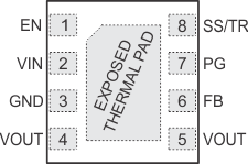
8-Pin µSiL Package
(SIL0008C Top View)
TPS82150 TPS82130_pinout.gif
space

Pin Functions

PIN I/O DESCRIPTION
NAME NO.
EN 1 I Enable pin. Pull High to enable the device. Pull Low to disable the device. This pin has an internal pull-down resistor of typically 400kΩ when the device is disabled.
VIN 2 PWR Input pin.
GND 3 Ground pin.
VOUT 4,5 PWR Output pin.
FB 6 I Feedback reference pin. An external resistor divider connected to this pin programs the output voltage.
PG 7 O Power good open drain output pin. A pull-up resistor can be connected to any voltage less than 6V. Leave it open if it is not used.
SS/TR 8 I Soft startup and voltage tracking pin. An external capacitor connected to this pin sets the internal reference voltage rising time.
Exposed Thermal Pad The exposed thermal pad must be connected to the GND pin. Must be soldered to achieve appropriate power dissipation and mechanical reliability.