JAJSJC6A December 2021 – June 2022 TPS92623-Q1
PRODUCTION DATA
- 1 特長
- 2 アプリケーション
- 3 概要
- 4 Revision History
- 5 Pin Configuration and Functions
- 6 Specifications
-
7 Detailed Description
- 7.1 Overview
- 7.2 Functional Block Diagram
- 7.3
Feature Description
- 7.3.1 Power Supply (SUPPLY)
- 7.3.2 Enable and Shutdown
- 7.3.3 Constant-Current Output and Setting (INx)
- 7.3.4 Thermal Sharing Resistor (OUTx and RESx)
- 7.3.5 PWM Control (PWMx)
- 7.3.6 Supply Control
- 7.3.7 Diagnostics
- 7.3.8 FAULT Bus Output with One-Fails-All-Fail
- 7.3.9 FAULT Table
- 7.3.10 LED Fault Summary
- 7.3.11 IO Pins Inner Connection
- 7.4 Device Functional Modes
- 8 Application and Implementation
- 9 Power Supply Recommendations
- 10Layout
- 11Device and Documentation Support
- 12Mechanical, Packaging, and Orderable Information
パッケージ・オプション
メカニカル・データ(パッケージ|ピン)
- PWP|16
サーマルパッド・メカニカル・データ
- PWP|16
発注情報
8.2.1.2 Detailed Design Procedure
Step 1: Determine the current sensing resistor, R(SNSx), by using Equation 4.
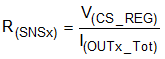
where
- V(CS_REG) = 150 mV (typical)
- I(OUTx_Tot) = 130 mA
According to design requirements, output current for each channel is same so that the R(SNS1) = R(SNS2) = R(SNS3) = 1.15 Ω. Two resistors in parallel can be used to achieve equivalent resistance when sense resistor is not a standard decade resistance value.
Step 2: Design the current distribution between I(OUTx) and I(RESx), and calculate the current sharing resistor, R(RESx), by using Equation 5. The R(RESx) value actually decides the current distribution for I(OUTx) path and I(RESx) path. TI recommends the current sharing resistor R(RESx) to consume 50% of the total current at typical supply operating voltage.
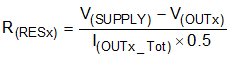
where
- V(SUPPLY) = 12 V (typical)
- I(OUTx_Tot) = 130 mA
The calculated result for R(RESx) resistor value including R(RES1), R(RES2)and R(RES3) is 85.4 Ω when V(OUTx) is typical 3 × 2.15 V = 6.45 V.
Step 3: Design the threshold voltage of SUPPLY to enable the LED open-circuit diagnostics, and calculate voltage divider resistor value for R1 and R2 on DIAGEN pin.
The maximum forward voltage of LED-string is 3 × 2.5 V = 7.5 V. To avoid the open-circuit fault reported in low-dropout operation conditions, additional headroom between SUPPLY and OUTx must be considered. TheTPS92623-Q1 device must disable open-circuit detection when the supply voltage is below LED-string maximum forward voltage plus V(OPEN_th_rising) and V(CS_REG). The voltage divider resistor, R1 and R2 value can be calculated by Equation 6.
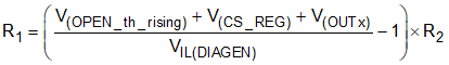
where
- V(OPEN_th_rising) = 420 mV (maximum)
- V(CS_REG) = 156 mV
- VIL(DIAGEN) = 1.045 V (minimum)
- R2 = 10 kΩ (recommended)
The calculated result for R1 is 67.3 kΩ when V(OUTx) maximum voltage is 7.5 V and V(CS_REG) is 156 mV.
Step 4: Design the threshold voltage of SUPPLY to turn on and off each channel of LED, and calculate voltage divider resistor value for R3 and R4 on PWM input pin.
The minimum forward voltage of LED string is 3 × 1.9 V = 5.7 V. To make sure the current output on each of LED-string is normal, each LED-string must be turned off when SUPPLY voltage is lower than LED minimum required forward voltage plus dropout voltage between INx to OUTx and V(CS_REG). The voltage divider resistor, R3 and R4 value can be calculated by Equation 7.
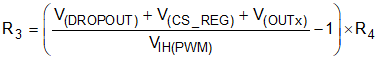
where
- V(DROPOUT) = 300 mV (typical)
- V(CS_REG) = 156 mV (maximum)
- VIH(PWM) = 1.26 V (maximum)
- R4 = 10 kΩ (recommended)
The calculated result for R3 is 38.9 kΩ when V(OUTx) minimum voltage is 5.7 V and V(CS_REG) is 156 mV.