JAJSIE5B December   2019  – September 2021 TPSM53603

PRODUCTION DATA  

  1. 特長
  2. アプリケーション
  3. 概要
  4. Revision History
  5. Pin Configuration and Functions
  6. Specifications
    1. 6.1 Absolute Maximum Ratings
    2. 6.2 ESD Ratings
    3. 6.3 Recommended Operating Conditions
    4. 6.4 Thermal Information
    5. 6.5 Electrical Characteristics
    6. 6.6 Typical Characteristics (VIN = 5 V)
    7. 6.7 Typical Characteristics (VIN = 12 V)
    8. 6.8 Typical Characteristics (VIN = 24 V)
    9. 6.9 Typical Characteristics (VIN = 36 V)
  7. Detailed Description
    1. 7.1 Overview
    2. 7.2 Functional Block Diagram
    3. 7.3 Feature Description
      1. 7.3.1  Adjusting the Output Voltage
      2. 7.3.2  Switching Frequency
      3. 7.3.3  Input Capacitors
      4. 7.3.4  Output Capacitors
      5. 7.3.5  Output On/Off Enable (EN)
      6. 7.3.6  Programmable Undervoltage Lockout (UVLO)
      7. 7.3.7  Power Good (PGOOD)
      8. 7.3.8  Light Load Operation
      9. 7.3.9  Voltage Dropout
      10. 7.3.10 Overcurrent Protection (OCP)
      11. 7.3.11 Thermal Shutdown
    4. 7.4 Device Functional Modes
      1. 7.4.1 Active Mode
      2. 7.4.2 Auto Mode
      3. 7.4.3 Shutdown Mode
  8. Application and Implementation
    1. 8.1 Application Information
    2. 8.2 Typical Application
      1. 8.2.1 Design Requirements
      2. 8.2.2 Detailed Design Procedure
        1. 8.2.2.1 Custom Design With WEBENCH® Tools
        2. 8.2.2.2 Output Voltage Setpoint
        3. 8.2.2.3 Input Capacitors
        4. 8.2.2.4 Output Capacitor Selection
      3. 8.2.3 Application Curves
  9. Power Supply Recommendations
  10. 10Layout
    1. 10.1 Layout Guidelines
    2. 10.2 Layout Examples
    3. 10.3 Theta JA versus PCB Area
    4. 10.4 Package Specifications
    5. 10.5 EMI
  11. 11Device and Documentation Support
    1. 11.1 Device Support
      1. 11.1.1 Third-Party Products Disclaimer
      2. 11.1.2 Development Support
        1. 11.1.2.1 Custom Design With WEBENCH® Tools
    2. 11.2 Documentation Support
      1. 11.2.1 Related Documentation
    3. 11.3 Receiving Notification of Documentation Updates
    4. 11.4 Support Resources
    5. 11.5 Trademarks
    6. 11.6 静電気放電に関する注意事項
    7. 11.7 Glossary
  12. 12Mechanical, Packaging, and Orderable Information

パッケージ・オプション

メカニカル・データ(パッケージ|ピン)
サーマルパッド・メカニカル・データ
発注情報

EMI

The TPSM53603 is compliant with EN55011 Class-B radiated emissions. Figure 10-5 and Figure 10-6 show typical examples of radiated emissions plots for the TPSM53603. The graphs include the plots of the antenna in the horizontal and vertical positions.

EMI plots were measured using the standard TPSM53603EVM with no input filter.
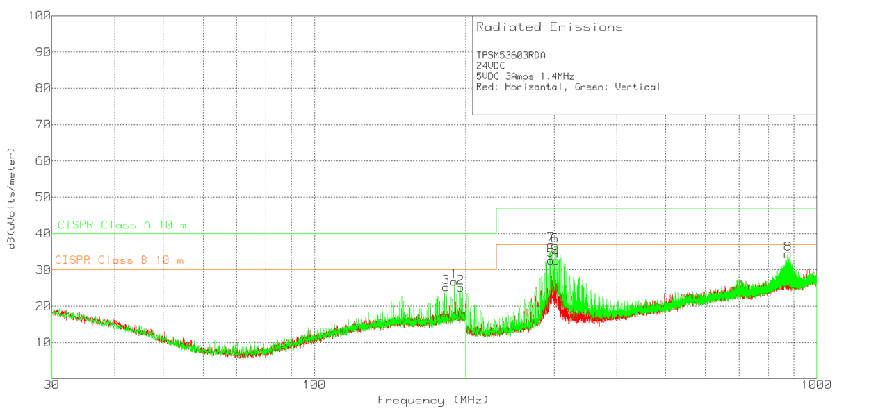
GUID-E9E52D74-EFE2-49AF-9055-AF06B89EFA74-low.gifFigure 10-5 Radiated Emissions 24-V Input, 5-V Output, 3-A Load
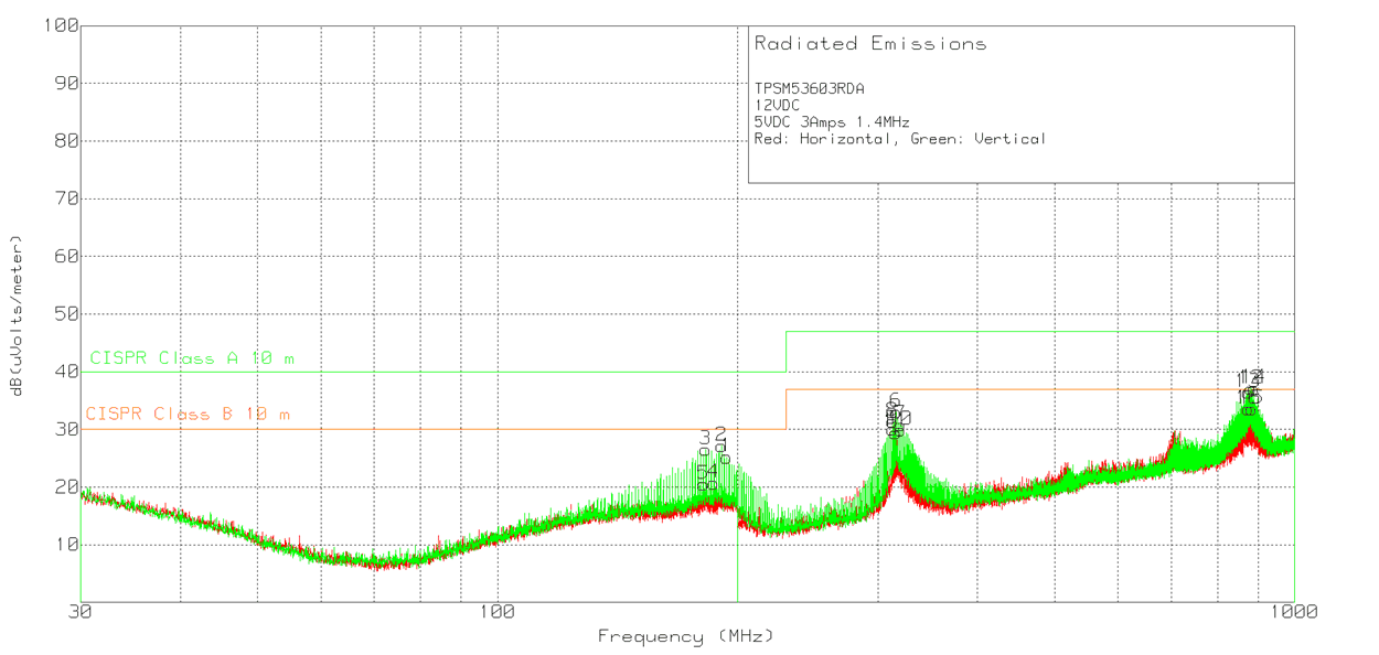
GUID-4882FCAB-F057-4D95-966C-49A30B7A5232-low.gifFigure 10-6 Radiated Emissions 12-V Input, 5-V Output, 3-A Load