JAJSHV7F August   2019  – November 2021 TPSM82821 , TPSM82821A , TPSM82822 , TPSM82822A , TPSM82823 , TPSM82823A

PRODUCTION DATA  

  1. 特長
  2. アプリケーション
  3. 概要
  4. Revision History
  5. Device Comparison Table
  6. Pin Configuration and Functions
  7. Specifications
    1. 7.1 Absolute Maximum Ratings
    2. 7.2 ESD Ratings
    3. 7.3 Recommended Operating Conditions
    4. 7.4 Thermal Information
    5. 7.5 Electrical Characteristics
    6. 7.6 Typical Characteristics
  8. Detailed Description
    1. 8.1 Overview
    2. 8.2 Functional Block Diagram
    3. 8.3 Feature Description
      1. 8.3.1 PWM and PSM Operation
      2. 8.3.2 Low Dropout Operation (100% Duty Cycle)
      3. 8.3.3 Soft Start-up
      4. 8.3.4 Switch Current Limit and Hiccup Short Circuit Protection
      5. 8.3.5 Undervoltage Lockout
      6. 8.3.6 Thermal Shutdown
    4. 8.4 Device Functional Modes
      1. 8.4.1 Enable and Disable
      2. 8.4.2 Output Discharge
      3. 8.4.3 Power Good Output
  9. Application and Implementation
    1. 9.1 Application Information
    2. 9.2 Typical Applications
      1. 9.2.1 1.8-V Output Application
        1. 9.2.1.1 Design Requirements
        2. 9.2.1.2 Detailed Design Procedure
          1. 9.2.1.2.1 Setting the Output Voltage
          2. 9.2.1.2.2 Feedforward capacitor
          3. 9.2.1.2.3 Input and Output Capacitor Selection
        3. 9.2.1.3 Application Performance Curves
          1. 9.2.1.3.1 TPSM82821 Performance Curves
          2. 9.2.1.3.2 TPSM82821A Performance Curves
          3. 9.2.1.3.3 TPSM82822 Performance Curves
          4. 9.2.1.3.4 TPSM82822A Performance Curves
          5. 9.2.1.3.5 TPSM82823 Performance Curves
          6. 9.2.1.3.6 TPSM82823A Performance Curves
  10. 10Power Supply Recommendations
  11. 11Layout
    1. 11.1 Layout Guidelines
    2. 11.2 Layout Example
      1. 11.2.1 Thermal Consideration
  12. 12Device and Documentation Support
    1. 12.1 Device Support
      1. 12.1.1 Third-Party Products Disclaimer
      2. 12.1.2 Development Support
        1. 12.1.2.1 Models and Simulators
    2. 12.2 Documentation Support
      1. 12.2.1 Related Documentation
    3. 12.3 Receiving Notification of Documentation Updates
    4. 12.4 Trademarks
    5. 12.5 Electrostatic Discharge Caution
    6. 12.6 Glossary

パッケージ・オプション

デバイスごとのパッケージ図は、PDF版データシートをご参照ください。

メカニカル・データ(パッケージ|ピン)
  • SIL|10
サーマルパッド・メカニカル・データ
発注情報
Setting the Output Voltage

Choose resistors R1 and R2 to set the output voltage within a range of 0.6 V to 4 V according to Equation 5. To keep the feedback (FB) net robust from noise, set R2 equal to or lower than 100 kΩ to have at least 6 µA of current in the voltage divider. Lower values of FB resistors achieve better noise immunity, and lower light load efficiency, as explained in the Design Considerations for a Resistive Feedback Divider in a DC/DC Converter Technical Brief.

Equation 5. GUID-D8EB4422-F47E-4C5A-AB18-B6C249537E62-low.gif
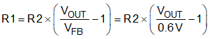
For devices with a fixed output voltage, the FB pin must be connected to VOUT. R1, R2 and C3 are not needed. The fixed output voltage devices have an internal feed forward capacitor.