JAJSHV7F August   2019  – November 2021 TPSM82821 , TPSM82821A , TPSM82822 , TPSM82822A , TPSM82823 , TPSM82823A

PRODUCTION DATA  

  1. 特長
  2. アプリケーション
  3. 概要
  4. Revision History
  5. Device Comparison Table
  6. Pin Configuration and Functions
  7. Specifications
    1. 7.1 Absolute Maximum Ratings
    2. 7.2 ESD Ratings
    3. 7.3 Recommended Operating Conditions
    4. 7.4 Thermal Information
    5. 7.5 Electrical Characteristics
    6. 7.6 Typical Characteristics
  8. Detailed Description
    1. 8.1 Overview
    2. 8.2 Functional Block Diagram
    3. 8.3 Feature Description
      1. 8.3.1 PWM and PSM Operation
      2. 8.3.2 Low Dropout Operation (100% Duty Cycle)
      3. 8.3.3 Soft Start-up
      4. 8.3.4 Switch Current Limit and Hiccup Short Circuit Protection
      5. 8.3.5 Undervoltage Lockout
      6. 8.3.6 Thermal Shutdown
    4. 8.4 Device Functional Modes
      1. 8.4.1 Enable and Disable
      2. 8.4.2 Output Discharge
      3. 8.4.3 Power Good Output
  9. Application and Implementation
    1. 9.1 Application Information
    2. 9.2 Typical Applications
      1. 9.2.1 1.8-V Output Application
        1. 9.2.1.1 Design Requirements
        2. 9.2.1.2 Detailed Design Procedure
          1. 9.2.1.2.1 Setting the Output Voltage
          2. 9.2.1.2.2 Feedforward capacitor
          3. 9.2.1.2.3 Input and Output Capacitor Selection
        3. 9.2.1.3 Application Performance Curves
          1. 9.2.1.3.1 TPSM82821 Performance Curves
          2. 9.2.1.3.2 TPSM82821A Performance Curves
          3. 9.2.1.3.3 TPSM82822 Performance Curves
          4. 9.2.1.3.4 TPSM82822A Performance Curves
          5. 9.2.1.3.5 TPSM82823 Performance Curves
          6. 9.2.1.3.6 TPSM82823A Performance Curves
  10. 10Power Supply Recommendations
  11. 11Layout
    1. 11.1 Layout Guidelines
    2. 11.2 Layout Example
      1. 11.2.1 Thermal Consideration
  12. 12Device and Documentation Support
    1. 12.1 Device Support
      1. 12.1.1 Third-Party Products Disclaimer
      2. 12.1.2 Development Support
        1. 12.1.2.1 Models and Simulators
    2. 12.2 Documentation Support
      1. 12.2.1 Related Documentation
    3. 12.3 Receiving Notification of Documentation Updates
    4. 12.4 Trademarks
    5. 12.5 Electrostatic Discharge Caution
    6. 12.6 Glossary

パッケージ・オプション

デバイスごとのパッケージ図は、PDF版データシートをご参照ください。

メカニカル・データ(パッケージ|ピン)
  • SIL|10
サーマルパッド・メカニカル・データ
発注情報

PWM and PSM Operation

The TPSM8282x includes a fixed on-time (tON) circuitry. This tON, in steady-state operation in PWM and PSM modes, is estimated as:

Equation 1. GUID-DCF43B93-D9F9-47FD-8EFB-EFC4A030D6FA-low.gif

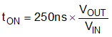
In PWM mode, the TPSM8282x operates with pulse width modulation in continuous conduction mode (CCM) with a tON shown in Equation 1 at medium and heavy load currents. A PWM switching frequency of typically 4 MHz is achieved by this tON circuitry.

To maintain high efficiency at light loads, the device enters power save mode seamlessly when the load current decreases. This happens when the load current becomes smaller than half the ripple current of the inductor. The output current at which this occurs can be approximated with the following equation:

Equation 2.

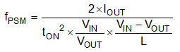
In PSM, the converter operates with a reduced switching frequency and with a minimum quiescent current to maintain high efficiency. The on time in PSM is also based on the same tON circuitry. The switching frequency in PSM is estimated as:

Equation 3. GUID-512BFC63-5CC5-4C47-AF99-7CF61929AFC8-low.gif

In PSM, the output voltage rises slightly above the nominal output voltage in PWM mode. This effect is reduced by increasing the output capacitance.

The forced PWM version of this device, the TPSM8282xA, does not enter PSM (power save mode) at light load currents and stays in CCM (continuous conduction mode) regardless of the output current in order to minimize the output ripple.