JAJSMI5A November 2021 – March 2022 TXU0102
PRODUCTION DATA
- 1 特長
- 2 アプリケーション
- 3 概要
- 4 Revision History
- 5 Related Products
- 6 Pin Configuration and Functions—TXU0102
-
7 Specifications
- 7.1 Absolute Maximum Ratings
- 7.2 ESD Ratings
- 7.3 Recommended Operating Conditions
- 7.4 Thermal Information
- 7.5 Electrical Characteristics
- 7.6 Switching Characteristics, VCCA = 1.2 ± 0.1 V
- 7.7 Switching Characteristics, VCCA = 1.5 ± 0.1 V
- 7.8 Switching Characteristics, VCCA = 1.8 ± 0.15 V
- 7.9 Switching Characteristics, VCCA = 2.5 ± 0.2 V
- 7.10 Switching Characteristics, VCCA = 3.3 ± 0.3 V
- 7.11 Switching Characteristics, VCCA = 5.0 ± 0.5 V
- 7.12 Operating Characteristics
- 7.13 Typical Characteristics
- 8 Parameter Measurement Information
-
9 Detailed Description
- 9.1 Overview
- 9.2 Functional Block Diagram
- 9.3
Feature Description
- 9.3.1 CMOS Schmitt-Trigger Inputs with Integrated Pulldowns
- 9.3.2 Control Logic (OE) with VCC(MIN) Circuitry
- 9.3.3 Balanced High-Drive CMOS Push-Pull Outputs
- 9.3.4 VCC Isolation and VCC Disconnect
- 9.3.5 Over-Voltage Tolerant Inputs
- 9.3.6 Glitch-Free Power Supply Sequencing
- 9.3.7 Negative Clamping Diodes
- 9.3.8 Fully Configurable Dual-Rail Design
- 9.3.9 Supports High-Speed Translation
- 9.4 Device Functional Modes
- 10Application and Implementation
- 11Power Supply Recommendations
- 12Layout
- 13Device and Documentation Support
- 14Mechanical, Packaging, and Orderable Information
パッケージ・オプション
デバイスごとのパッケージ図は、PDF版データシートをご参照ください。
メカニカル・データ(パッケージ|ピン)
- DCU|8
- DTM|8
- DTT|8
サーマルパッド・メカニカル・データ
発注情報
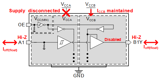
9.3.4 VCC Isolation and VCC Disconnect
The outputs for this device are disabled and enter a high-impedance state when either supply is <100 mV or left floating (disconnected), with the complementary supply within recommended operating conditions. It is recommended that the inputs are kept low before floating (disconnecting) either supply.
The ICCx(floating) in the Electrical Characteristics specifies the maximum supply current. The Ioff(float) in the Electrical Characteristics specifies the maximum leakage into or out of any input or output pin on the device.
 Figure 9-1 VCC Disconnect
Feature