JAJSEQ5A August 2017 – February 2018 UCC24612
PRODUCTION DATA.
- 1 特長
- 2 アプリケーション
- 3 概要
- 4 改訂履歴
- 5 Pin Configuration and Functions
- 6 Specifications
- 7 Detailed Description
- 8 Application and Implementation
- 9 Power Supply Recommendations
- 10PCB Layout
- 11デバイスおよびドキュメントのサポート
- 12メカニカル、パッケージ、および注文情報
7.3.1 Power Management
The UCC24612 SR controller is powered from REG pin through the internal linear regulator between VDD pin and REG pin. This configuration allows optimal design of the gate driver stage to achieve fast driving speed, low driving loss and higher noise immunity.
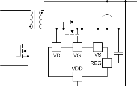
In low-side SR configuration, as shown in Figure 13, the UCC24612 is powered from the output voltage directly.
 Figure 13. UCC24612 Used in Low-side SR Configuration
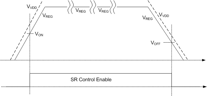
During start up, the output voltage rises from zero. With the rising of output voltage, the internal linear regulator operates in a pass-through mode, and the REG pin voltage rises together with the output voltage. The UVLO function of UCC24612 monitors the voltage on the REG pin instead of the VDD pin. Before REG pin voltage rises above UVLO on threshold VREGON, UCC24612 consumes the minimum current IVDDSTART. Once the REG voltage rises above VREGON, the device starts to consume the full operating current and controls the switching of the SR MOSFET.
When VDD voltage is above 9.5 V, the internal linear regulator operates in regulator mode. The REG pin is well regulated at 9.5 V. This voltage level is chosen to give a good compromise between SR conduction loss and gate drive loss. The internal regulator is rated at 10 mA of average load regulation capability for higher switching frequency operation. It is required to have a sufficient bypass capacitor on the REG pin to ensure stable operation of the linear regulator. A 2.2-µF bypass capacitor is recommended.
When VDD voltage is below 9.5 V, the internal linear regulator operates in pass-through mode. Depending on the load current, the regulator has a voltage drop of approximately 0.2 V. The UCC24612 continues to operate during this mode until the REG pin voltage drops below UVLO turn off level VREGOFF.
A typical timing diagram of VDD and REG pin voltage can be found in Figure 14.
 Figure 14. Timing Diagram for VDD and REG in Low-side SR Configuration
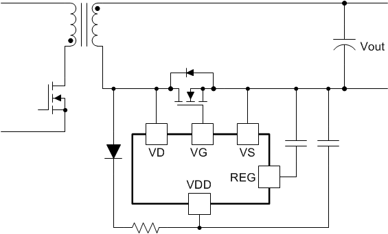
In some applications, such as USB chargers, the converter is required to deliver the full output current when the output is over loaded and output voltage drops below the regulation level. In 5-V applications, the output voltage could drop too low to adequately turn on the SR. In this case, the UCC24612 can be powered through a simple external R-C-D circuit, as shown in Figure 15. Due to the wide voltage range handling capability, this simple circuit provides power from the SR drain voltage. Even though this method easily powers up the device, this is a very inefficient way of powering the controller. A more efficient way would be to use an auxiliary winding to provide the power.
 Figure 15. UCC24612 Used in Low-side and Low Output Voltage Condition
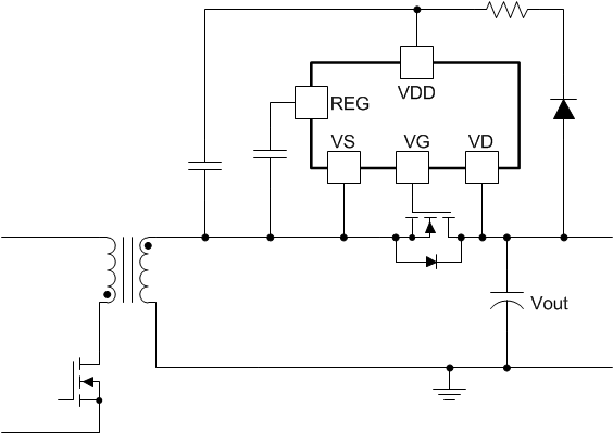
The same biasing method can also maintain the SR controller operation in high-side SR configuration, as shown in Figure 16. More details about biasing UCC24612 can be found in Power Supply Recommendations.
 Figure 16. UCC24612 Used in High-Side SR Configuration