JAJSEQ5A August 2017 – February 2018 UCC24612
PRODUCTION DATA.
- 1 特長
- 2 アプリケーション
- 3 概要
- 4 改訂履歴
- 5 Pin Configuration and Functions
- 6 Specifications
- 7 Detailed Description
- 8 Application and Implementation
- 9 Power Supply Recommendations
- 10PCB Layout
- 11デバイスおよびドキュメントのサポート
- 12メカニカル、パッケージ、および注文情報
7.3.3.2 Turn-Off Blanking Timer
When the converter operates in discontinuous conduction mode (DCM) or burst mode, after SR turn-off, there is a large parasitic DCM ring caused by the primary inductance and the switch node capacitance. For the first couple of ringing cycles, there is a possibility that the drain voltage can resonate below the SR turn-on threshold. The SR could be falsely turned on at these instances and introduce extra loss and EMI noise.
The DCM ringing is blanked by an off blanking timer. It is often called minimum off-time. Due to the range of switching frequencies and power levels, the parasitic ringing frequency can vary substantially. The programmable off blanking timer provides maximum flexibility for the circuit design and avoids false triggering. However, there are some limitations associated with this method. Firstly, the need for a programming pin can force a higher pin count package, which increases the overall cost and difficulty of layout. Secondly, a fixed off blanking timer might not work well for the entire range of line and load conditions. For example, for a quasi-resonant (QR) Flyback, in light load mode, it enters DCM operation. In this case, the off blanking timer should be long to avoid DCM ringing induced SR false turn on. However, at high input voltage, when the converter operates in QR mode, the primary side MOSFET conduction time is quite short, and long minimum off-time might cut into the conduction time of the SR, introducing extra conduction loss.
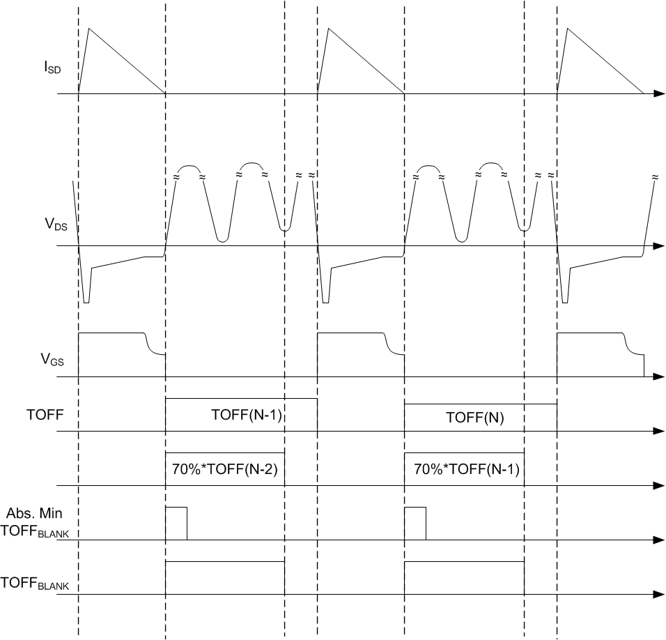
In UCC24612, instead of a fixed off blanking timer, an adaptive off blanking timer is used to blank the parasitic ringing and avoid false turn-on. The off blanking timer TOFFblankis determined by the maximum value of three timings, the absolute minimum off blanking time of 400 ns (tOFF_ABSMIN), the recorded DCM ring cycle time tDCM and the previous cycle's SR off time tOFF.
UCC24612 sets up the off blanking timer based on the previous cycle SR off time. By choosing 70% of previous switching cycle's SR off time, the off blanking timer is maximized to prevent any false triggering.
However, the off blanking timer minimum value is clamped by the 400-ns absolute minimum value and recorded DCM ringing cycle.
The adaptive off-time blanking operation principle is illustrated in Figure 20.
 Figure 20. Operation Principle of Adaptive off-blanking
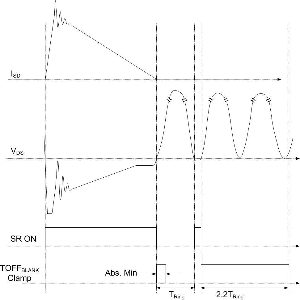
After SR turn-off, if the off blanking time is not sufficient, the SR could be turned on again by a DCM ring. Because of the DCM ring, the SR conduction time is limited by its minimum on-time. By looking at the SR conduction time and comparing it with the minimum on time, UCC24612 is able to determine if the conduction is a real SR conduction or a false turn on triggered by the DCM ring. A real SR conduction should demand the conduction time longer than the minimum on-time. Once the false turn-on is captured, the time duration between previous SR turn-off and the SR false turn-on is recorded as the DCM ring cycle. For the next switching cycle, the off blanking timer is clamped to 2.2 times of the recorded DCM ring cycle. This clamp replaces the 350-ns clamp as the new minimum clamp for the adaptive-off blanking. This adaptive off-blanking timer allows UCC24612 achieving the noise immunity without a dedicated programming pin. The DCM ring clamp is illustrated in Figure 21.
 Figure 21. Adaptive Off-Time Blanking with DCM Ring Clamp
For some conditions, as mentioned earlier, the off blanking timer suitable for DCM operation might be too long for high-line QR operation. In this case, the off blanking timer clamp needs to be reset to the correct value. UCC24612 continuously monitors the SR body diode conduction time during minimum off-time. If the body diode conduction time is longer than the minimum on-time, this means the minimum off blanking time clamp setting is too long and needs to be reduced. UCC24612 resets the minimum off blanking time clamp to the absolute minimum of 400 ns to allow full conduction of the SR on the subsequent cycles.
If for any reason the off blanking time expires after the SR body diode conduction, the SR turn-on is skipped for the switching cycle. This is because when the SR conducts, it conducts with a minimum on-time, if the blanking time expires at the end of the SR conduction time and converter operates in the CCM condition, there is a good chance to cause shoot-through and endanger the converter.
The off blanking time has a maximum value of tOFF_MAX at 3.68 µs.