JAJSEQ5A August 2017 – February 2018 UCC24612
PRODUCTION DATA.
- 1 特長
- 2 アプリケーション
- 3 概要
- 4 改訂履歴
- 5 Pin Configuration and Functions
- 6 Specifications
- 7 Detailed Description
- 8 Application and Implementation
- 9 Power Supply Recommendations
- 10PCB Layout
- 11デバイスおよびドキュメントのサポート
- 12メカニカル、パッケージ、および注文情報
9 Power Supply Recommendations
UCC24612 internal circuits are powered from the REG pin only. There is an internal LDO between VDD pin and REG pin to provide a well-regulated REG pin voltage when VDD voltage is above 9.5 V. This allows the device to have better bypassing and better gate driver performance.
It is important to have sufficient bypass cap on REG pin. A minimum of 1.5-µF bypass capacitor is required. When the average gate charge current is higher than 5mA, it is required to have at least 2.2-µF bypass capacitor on REG pin.
VDD pin is the main power source of the device. The voltage on VDD pin should be kept between 4.5 V and 28 V for normal operation. Refer to the electrical characteristics table for the tolerances on the REG pin UVLO ON and OFF levels.
When UCC24612 is used in low-side SR configuration, VDD can be directly tied to the output voltage if the output voltage is between 4.5 V to 28 V.
When the UCC24612 is used in high-side SR configuration, VDD can be powered through three different ways, with a trade off between cost and performance.
- Power the device through secondary-side auxiliary winding
- Power the device through simple R-C filter
- Power the device through depletion mode FET
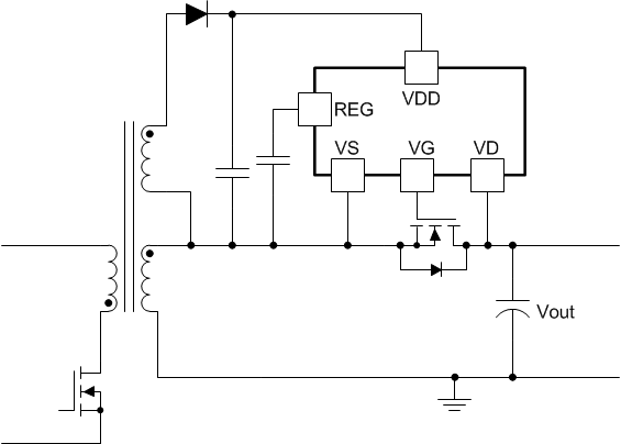
By using the secondary-side auxiliary winding, as shown in Figure 32, UCC24612 is equivalently powered by the output voltage because of the transformer coupling effect. This provides the best efficiency solution. However, this solution is often limited by the transformer construction and cost constraints.
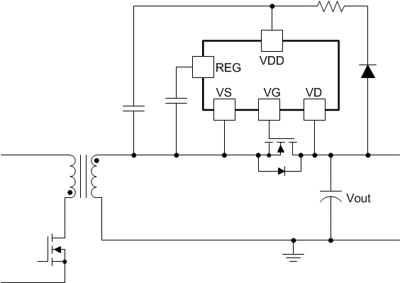
The UCC24612 can be powered by using a diode and RC filter on VDD pin, as shown in Figure 33. This allows the device to get power from the SR drain voltage. Due to the wide range of VD voltage variation (for example, VD voltage is the sum of reflected input voltage and output voltage in Flyback converter), this may not be acceptable for some applications due to the limit of absolute maximum VDD voltage rating. However, this provides a simple and low cost solution.
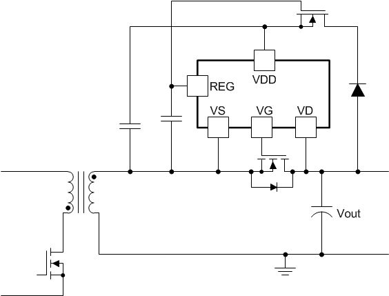
A more universal solution without changing the transformer is to provide the VDD through SR drain using a diode and depletion mode MOSFET, as shown in Figure 34. This allows a well regulated VDD voltage throughout the entire operation range of the converter. Even though it still reducess the efficiency because the device is powered up from a high voltage source, this provides a simple solution without changing the transformer design.
The three different configurations are summarized in Figure 32, Figure 33 and Figure 34.
 Figure 32. Power UCC24612 Using Auxiliary Winding
 Figure 33. Power UCC24612 Using R-C-D
 Figure 34. Powering UCC24612 Using Depletion Mode MOSFET