JAJSEQ5A August 2017 – February 2018 UCC24612
PRODUCTION DATA.
- 1 特長
- 2 アプリケーション
- 3 概要
- 4 改訂履歴
- 5 Pin Configuration and Functions
- 6 Specifications
- 7 Detailed Description
- 8 Application and Implementation
- 9 Power Supply Recommendations
- 10PCB Layout
- 11デバイスおよびドキュメントのサポート
- 12メカニカル、パッケージ、および注文情報
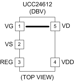
5 Pin Configuration and Functions
5-Pin SOT-23

Pin Functions
| PIN | I/O | DESCRIPTION | |
|---|---|---|---|
| NAME | NO. | ||
| REG | 3 | O |
REG is the device bias pin. An internal linear regulator from VDD to REG generates a well regulated 9.5-V voltage. It is recommend to put a 2.2-µF bypass capacitor from REG pin to VS pin. |
| VD | 5 | I |
MOSFET drain voltage sensing input. Connect this pin to SR MOSFET drain pin. The layout should avoid sharing the VD pin trace with the power path to minimize the impact of parasitic inductance. |
| VDD | 4 | I |
Internal linear regulator input. Connect this pin to the output voltage when in low-side SR configuration. Use R-C-D circuit or other circuits to generate bias voltage from SR MOSFET drain when using high-side SR configuration, referring to Power Supply Recommendations for details. |
| VG | 1 | O |
VG (controlled MOSFET gate drive), connect VG to the gate of the controlled MOSFET through a small series resistor using short PC board tracks to achieve optimal switching performance. The VG output can achieve >1-A peak source current when High and >4-A peak sink current when Low when connected to a large N-channel power MOSFET. Due to the weak internal pull up after initial fast turn on, avoid putting a resistor less than 50 kΩ between VG to VS . |
| VS | 2 | - |
VS is the internal ground reference of the UCC24612. It is also used to sense the voltage drop across the SR MOSFET. The layout should avoid sharing the VS pin trace with the power path to minimize the impact of parasitic inductance. |