JAJSFV5C July 2018 – March 2022 UCC24624
PRODUCTION DATA
- 1 特長
- 2 アプリケーション
- 3 概要
- 4 Revision History
- 5 概要 (続き)
- 6 Pin Configuration and Functions
- 7 Specifications
- 8 Detailed Description
- 9 Application and Implementation
- 10Power Supply Recommendations
- 11Layout
- 12Device and Documentation Support
10 Power Supply Recommendations
UCC24624 internal circuits are powered from REG pin only. There is an internal linear regulator between VDD pin and REG pin to provide a well-regulated REG pin voltage when VDD voltage is above 11 V. This allows the device to have better bypassing and better gate driver performance.
It is important to keep the sufficient bypass cap on REG pin. A minimum of 1-μF bypass capacitor is required. When the gate charge current is higher than 5 mA, it is required to have at least 2.2-μF bypass capacitor on REG pin.
VDD pin is the main power source of the device. Keep the voltage on VDD pin between 4.25 V and 26 V for normal operation. Refer to Section 7.5 for the tolerances on the REG pin UVLO ON and OFF levels. It is recommended to power up the VDD from the output of LLC as shown in Figure 8-1. It will make sure one of the drain-to-source voltages (VD1 or VD2) will switch above VTHARM before REG pin voltage reaches VREGON threshold for the proper switching of VG1 and VG2. Other power up methods are also possible (Figure 10-1).
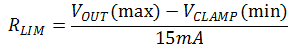
For the applications where LLC output voltage is higher than 24.75 V, an external resistor between LLC output voltage and UCC24624 can be used to allow internal clamp circuit keeping the VDD voltage below its recommended maximum voltage rating, as shown in Figure 8-3. The series resistor can be calculated as in Equation 7. In Equation 7, VOUT(max) is the maximum output voltage of LLC converter, including its transient conditions, VCLAMP(min) is the minimum clamping voltage considering tolerance, and ILIM is the maximum current allowed by the clamping circuit of 15 mA.
After the resistor is inserted, calculate the minimum voltage on VDD to ensure sufficient voltage on VDD for the SR driving. The voltage on VDD based on RLIM can be calculated as Equation 8. The VDD voltage under this condition must be higher than desired minimum SR driving voltage. In this equation, VOUT is the nominal output voltage, RLIM is the current limiting resistor value. Qg is the SR gate charge for each SR MOSFET and fSW is the maximum switching frequency of LLC converter.

If the output voltage is higher than 36 V, or no suitable current limit resistor RLIM can be selected or incase, the auxiliary winding can be used to power up the UCC24624. The circuit diagram of powering UCC24624 using auxiliary winding is shown in Figure 10-1. Other option would be to use a linear regulator to create bias power from the output voltage directly. But this is a less efficient solution.
 Figure 10-1 Powering UCC24624 Using
Auxiliary Winding
Figure 10-1 Powering UCC24624 Using
Auxiliary Winding