JAJSFV5C July 2018 – March 2022 UCC24624
PRODUCTION DATA
- 1 特長
- 2 アプリケーション
- 3 概要
- 4 Revision History
- 5 概要 (続き)
- 6 Pin Configuration and Functions
- 7 Specifications
- 8 Detailed Description
- 9 Application and Implementation
- 10Power Supply Recommendations
- 11Layout
- 12Device and Documentation Support
8.3.3 Turn-off Threshold Adjustment
When SR MOSFETs are implemented in LLC converters, they are often turned off too early, which creates long body diode conduction times. This results in more power loss, lower efficiency, and higher thermal stress.
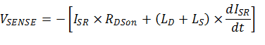
The SR MOSFET early turn off is caused by the parasitic inductance in the SR voltage sensing path. As illustrated in Figure 8-5, the VDS voltage sensed by the synchronous rectifier controller (VSENSE) is the combination of the MOSFET on-state resistor voltage drop VSR, together with the voltage drops on parasitic inductors LD and LS. A better layout approach can minimize these parasitic inductors. However, the minimum value it can achieve is the package inductance of the SR MOSFET. With different packages, this parasitic inductance could vary from 2 to 10 nH.
 Figure 8-5 SR Controller Sensed Voltage
The overall sensed voltage can be represented by Equation 1.
Because of the sinusoidal current shape and high output current, the current slope (di/dt) creates a significant voltage drop across the package inductance. This causes the SR controller to detect a smaller voltage drop and turn off the SR MOSFET early.
To overcome this issue, UCC24624 implements several techniques.
First, the proportional gate drive feature is implemented. As discussed earlier, the proportional gate drive reduces the SR MOSFET gate drive voltage when the SR current is small, and increases its voltage drop. This increased voltage drop could overwhelm the offset voltage introduced by the package inductance. Thus the SR MOSFET conduction time is extended.
Second, the turn-off threshold is set at 10.5 mV, instead of typically being set as a negative threshold. Because of the high di/dt and unavoidable SR package inductance, positive voltage is always expected at zero SR current. The positive turn-off threshold allows the SR MOSFET to continue conduction toward the end of the intended conduction period without the concern of causing negative SR current because of anticipating the positive offset voltage on the package inductances.
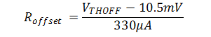
Last, UCC24624 also allows the user to further increase the turn-off threshold to accommodate higher parasitic inductance MOSFET packages, such as TO-220 packages. As illustrated in Figure 8-6, UCC24624 has an internal current source that flows out of the VSS pin. By connecting a resistor from the VSS pin to the SR MOSFET source, the voltage drop across the external resistor increases the turn-off threshold. This increased turn-off threshold makes it more suitable for TO-220 packages. Less than 70-mV offset is recommended. When using the low inductance MOSFET packages, such as SON5x6, the external resistor is not needed because the proportional gate drive alone can take care of the offset caused by the smaller package inductance.
To ensure normal system operation, VSS pin must never be kept open.
 Figure 8-6 Adjustable Turn-off Threshold
The internal current source is at 330 µA and the external offset resistor value is recommended to be less than 212 Ω. The offset resistor Roffset can be calculated by using Equation 2 with the desired turn-off threshold VTHOFF.
This added offset voltage only changes the SR turn-off threshold, while the proportional gate drive threshold remains the same.