JAJSC45C August 2013 – October 2015 UCC27211A
PRODUCTION DATA.
- 1 特長
- 2 アプリケーション
- 3 概要
- 4 改訂履歴
- 5 Description (continued)
- 6 Pin Configuration and Functions
-
7 Specifications
- 7.1 Absolute Maximum Ratings
- 7.2 ESD Ratings
- 7.3 Recommended Operating Conditions
- 7.4 Thermal Information
- 7.5 Electrical Characteristics
- 7.6 Switching Characteristics: Propagation Delays
- 7.7 Switching Characteristics: Delay Matching
- 7.8 Switching Characteristics: Output Rise and Fall Time
- 7.9 Switching Characteristics: Miscellaneous
- 7.10 Typical Characteristics
- 8 Detailed Description
- 9 Application and Implementation
- 10Power Supply Recommendations
- 11Layout
- 12デバイスおよびドキュメントのサポート
- 13メカニカル、パッケージ、および注文情報
パッケージ・オプション
メカニカル・データ(パッケージ|ピン)
- DRM|8
サーマルパッド・メカニカル・データ
- DRM|8
発注情報
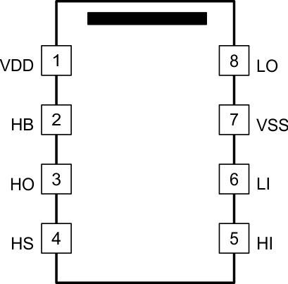
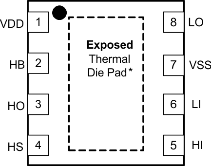
6 Pin Configuration and Functions
D Package
8-Pin SOIC
Top View

DRM Package
8-Pin VSON
Top View

Pin Functions
| PIN | I/O | DESCRIPTION | |
|---|---|---|---|
| NAME | NO. | ||
| HB | 2 | P | High-side bootstrap supply. The bootstrap diode is on-chip but the external bootstrap capacitor is required. Connect positive side of the bootstrap capacitor to this pin. Typical range of HB bypass capacitor is 0.022 µF to 0.1 µF. The capacitor value is dependant on the gate charge of the high-side MOSFET and must also be selected based on speed and ripple criteria. |
| HI | 5 | I | High-side input.(1) |
| HO | 3 | O | High-side output. Connect to the gate of the high-side power MOSFET. |
| HS | 4 | P | High-side source connection. Connect to source of high-side power MOSFET. Connect the negative side of bootstrap capacitor to this pin. |
| LI | 6 | I | Low-side input.(1) |
| LO | 8 | O | Low-side output. Connect to the gate of the low-side power MOSFET. |
| VDD | 1 | P | Positive supply to the lower-gate driver. De-couple this pin to VSS (GND). Typical decoupling capacitor range is 0.22 µF to 4.7 µF (See (2)). |
| VSS | 7 | — | Negative supply terminal for the device that is generally grounded. |
| Thermal pad(3) | — | Utilized on the DRM package only. Electrically referenced to VSS (GND). Connect to a large thermal mass trace or GND plane to dramatically improve thermal performance. | |
(1) HI or LI input is assumed to connect to a low impedance source signal. The source output impedance is assumed less than 100 Ω. If the source impedance is greater than 100 Ω, add a bypassing capacitor, each, between HI and VSS and between LI and VSS. The added capacitor value depends on the noise levels presented on the pins, typically from 1 nF to 10 nF should be effective to eliminate the possible noise effect. When noise is present on two pins, HI or LI, the effect is to cause HO and LO malfunctions to have wrong logic outputs.
(2) For cold temperature applications TI recommends the upper capacitance range. Follow the Layout Guidelines for PCB layout.
(3) The thermal pad is not directly connected to any leads of the package; however, it is electrically and thermally connected to the substrate which is the ground of the device.