SLUS769D July 2013 – December 2016 UCC28910 , UCC28911
PRODUCTION DATA.
- 1 Features
- 2 Applications
- 3 Description
- 4 Simplified Schematic
- 5 Revision History
- 6 Device Comparison Table
- 7 Pin Configuration and Functions
- 8 Detailed Pin Description
- 9 Specifications
-
10Detailed Description
- 10.1 Overview
- 10.2 Functional Block Diagram
- 10.3 Feature Description
- 10.4 Device Functional Modes
-
11Applications and Implementation
- 11.1 Application Information
- 11.2
Typical Application
- 11.2.1
Battery Charger, 5 V, 6 W
- 11.2.1.1 Design Requirements
- 11.2.1.2
Detailed Design Procedure
- 11.2.1.2.1 Power Handling Curves
- 11.2.1.2.2 Input Stage Design and Bulk Capacitance
- 11.2.1.2.3 Transformer Turns Ratio
- 11.2.1.2.4 Output Capacitance
- 11.2.1.2.5 VDD Capacitance, CVDD
- 11.2.1.2.6 VS Resistor Divider
- 11.2.1.2.7 RVDD Resistor and Turn Ratio
- 11.2.1.2.8 Transformer Input Power
- 11.2.1.2.9 RIPK Value
- 11.2.1.2.10 Transformer Primary Inductance Value
- 11.2.1.2.11 Pre-Load
- 11.2.1.2.12 DRAIN Voltage Clamp Circuit
- 11.2.2 Application Curves
- 11.2.3 Multi-Output Converter with UCC2891x Devices
- 11.2.4 Do’s and Don'ts
- 11.2.1
Battery Charger, 5 V, 6 W
- 12Power Supply Recommendations
- 13Layout
- 14Device and Documentation Support
- 15Mechanical, Packaging, and Orderable Information
8 Detailed Pin Description
8.1 VDD (Device Voltage Supply)
The VDD pin is connected to a bypass capacitor to ground and typically to a rectifier diode connected to the auxiliary winding. The VDD turn on UVLO threshold is 9.5 V (VDDON typical) and turn off UVLO threshold is 6.5 V (VDDOFF typical). The pin is provided with an internal clamp that prevents the voltage from exceeding the absolute maximum rating of the pin. The internal clamp cannot absorb currents higher than 10 mA (see IVDD(clp) in Absolute Maximum Ratings). To avoid damaging the device, when the clamp flowing current exceeds 6 mA (IDDCLP_OC typical) the device stops switching. The VDD pin operating range is then from 7 V (VDDOFF maximum) up to 26 V (VDDCLAMP minimum). The USB charging specification requires that the output current operates in constant current mode from 5 V to a minimum of 2 V; this is easily achieved with a nominal VDD of approximately 17 V. Set NAS (auxiliary-to-secondary windings turn ratio) to 17 V / (VOUT + VF) where VF is the voltage drop on the output diode at low current. The additional VDD headroom up to the clamp allows for VDD to rise due to the leakage energy delivered to the VDD in high-load conditions.
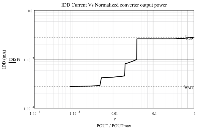
The current consumption of the device depends upon the operating condition. The graph below shows the current consumption as a function of normalized converter output power.
 Figure 1. VDD Current Consumption
8.2 GND (Ground)
The device is provided with three pins, shorted together, that are used as external ground reference to the controller for analog signal reference. The three pins also function to pull out the heat caused by the power dissipation of the internal power FET. Place the VDD bypass capacitor close to GND and VDD with short traces to minimize noise on the VS and IPK signal pins.
8.3 VS (Voltage Sense)
The VS pin is connected to a resistor divider from the auxiliary winding to ground. The VS input provides three functions.
- It provides output voltage information to the voltage control Loop. The output voltage feedback information is sampled at the end of the transformer secondary current demagnetization time to provide an accurate representation of the output voltage.
- It also provides timing information to achieve valley switching and the duty cycle of the secondary transformer current is determined by the waveform on the VS pin.
- It samples the bulk capacitor input voltage providing under-voltage shutdown.
The data provided in 1. and 2. are sensed during the MOSFET off-time; 3. is performed during the MOSFET on-time when the auxiliary-winding voltage is negative.
Connected between VS pin and the auxiliary winding there is the resistance RS1. During MOSFET on-time the auxiliary voltage is negative and proportional to the converter input voltage. The voltage on VS pin is clamped to GND and through the resistance RS1. During the on-time, the current sourced from the VS pin, proportional to converter input voltage and inversely proportional to resistance RS1, is sensed by the device. For the under-voltage function, the enable threshold on VS current is 210 μA and the disable threshold is 75 μA.
The resistor values for RS1 and RS2 can be determined by the equations below.

where

where
8.4 IPK (Set the Maximum DRAIN Current Peak)
A resistance (RIPK) connected between IPK pin and GND sets the maximum value of the power FET peak current, ID_PK(max). A current, ISENSE, proportional to the power FET current, comes out from the IPK pin during power FET on time. The voltage across RIPK is fed to the PWM comparator and establish to switch off the power FET according to the following equation:

where
- VCSTE(max) is the equivalent current sense threshold (see Electrical Characteristics table).
If the IPK pin is shorted to GND (RIPK = 0), the peak current is automatically set to ID_PEAK(max), 600 mA for UCC28910, or 700 mA for UCC28911.
A test is performed at device start up to check whether the IPK pin is shorted to GND or the RIPK is present. If RIPK is less than RIPK_SHORT (maximum), the device interprets it as a short (RIPK = 0) and the DRAIN peak current is set to ID_PEAK(max). Otherwise, if RIPK is greater than RIPK(min) (minimum), the device sets the peak current DRAIN according to the previous equation. A value of RIPK that is in between the before said values is not allowed since the value of the peak current may be selected using either of the two sense resistances: the internal sense resistance and RIPK.
8.5 DRAIN
The DRAIN pin is connected to the DRAIN of the internal power FET. This pin also provides current to the high voltage current source at start up.