JAJSN98E May 2020 – February 2024 UCC5350-Q1
PRODUCTION DATA
- 1
- 1 特長
- 2 アプリケーション
- 3 概要
- 4 概要 (続き)
- 5 Pin Configuration and Function
-
6 Specifications
- 6.1 Absolute Maximum Ratings
- 6.2 ESD Ratings
- 6.3 Recommended Operating Conditions
- 6.4 Thermal Information
- 6.5 Power Ratings
- 6.6 Insulation Specifications for D Package
- 6.7 Insulation Specifications for DWV Package
- 6.8 Safety-Related Certifications For D Package
- 6.9 Safety-Related Certifications For DWV Package
- 6.10 Safety Limiting Values
- 6.11 Electrical Characteristics
- 6.12 Switching Characteristics
- 6.13 Insulation Characteristics Curves
- 6.14 Typical Characteristics
- 7 Parameter Measurement Information
- 8 Detailed Description
- 9 Application and Implementation
- 10Power Supply Recommendations
- 11Layout
- 12Device and Documentation Support
- 13Revision History
- 14Mechanical, Packaging, and Orderable Information
パッケージ・オプション
メカニカル・データ(パッケージ|ピン)
サーマルパッド・メカニカル・データ
発注情報
11.2 Layout Example
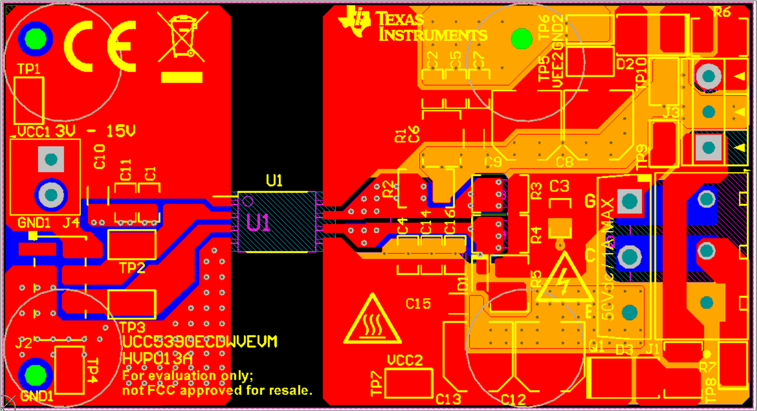
Figure 11-1 shows a PCB layout example with the signals and key components labeled. The UCC5390ECDWV evaluation module (EVM) is given as an example, available in the same DWV package as the UCC5350-Q1. The UCC5390EC has a split emitter versus Miller clamp so although the layout is not exactly the same, general guidelines and practices still apply. The evaluation board can be configured for the Miller clamp version, as well, as described in the UCC5390ECDWV Isolated Gate Driver Evaluation Module User's Guide.

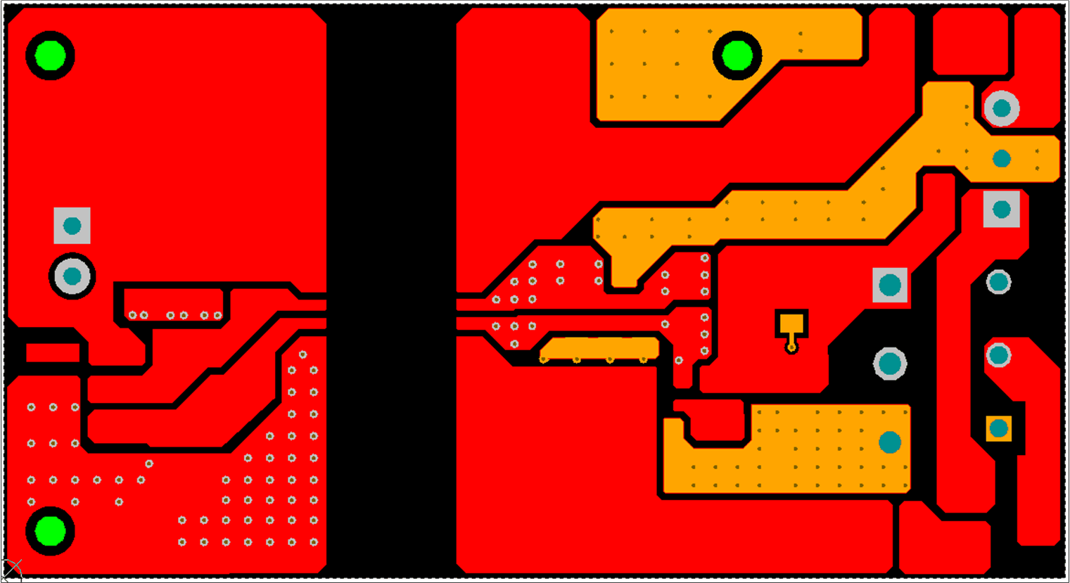
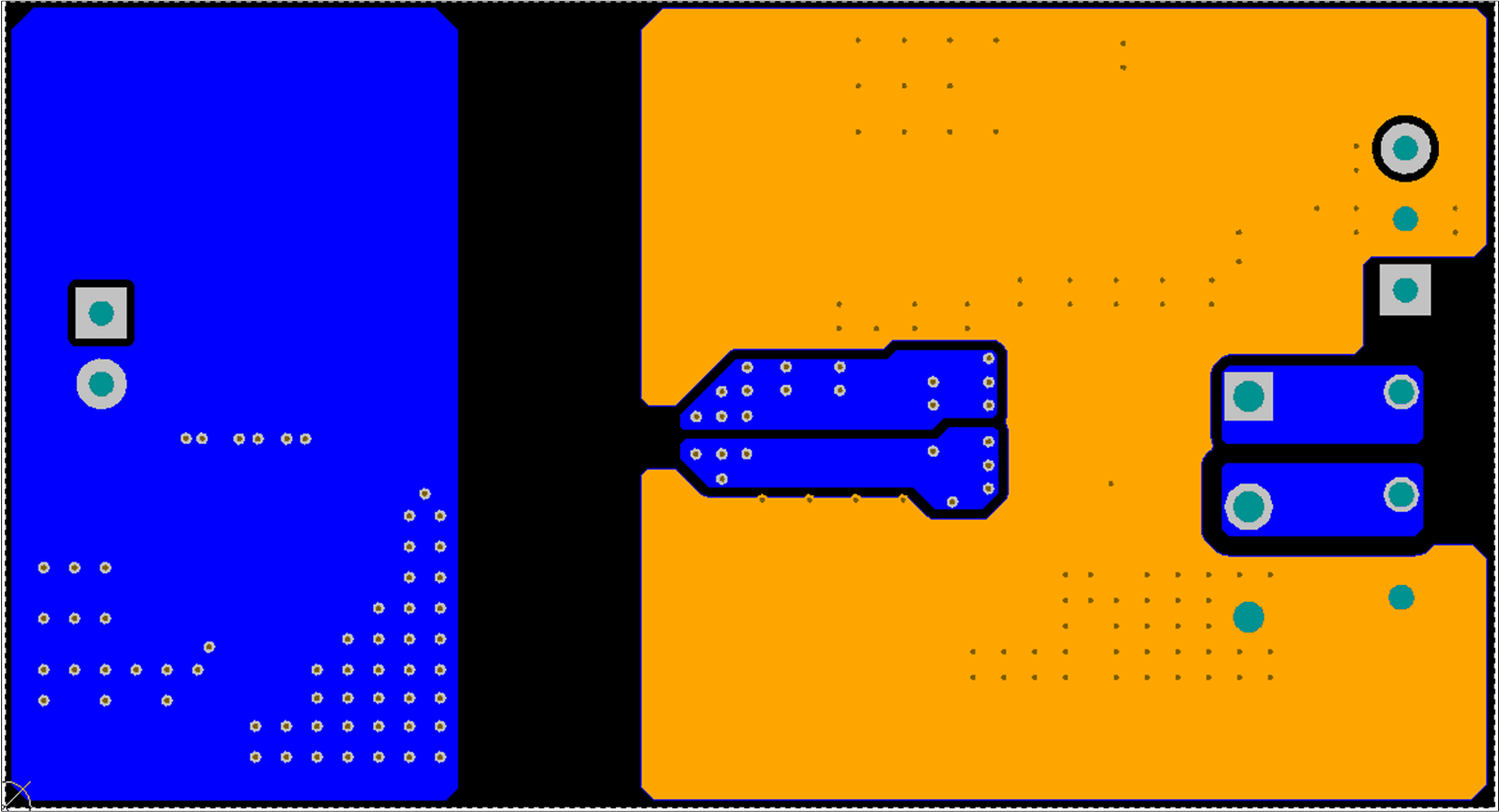
Figure 11-2 and Figure 11-3 show the top and bottom layer traces and copper.
 Figure 11-2 Top-Layer Traces and
Copper
 Figure 11-3 Bottom-Layer Traces and Copper
(Flipped)
Figure 11-3 Bottom-Layer Traces and Copper
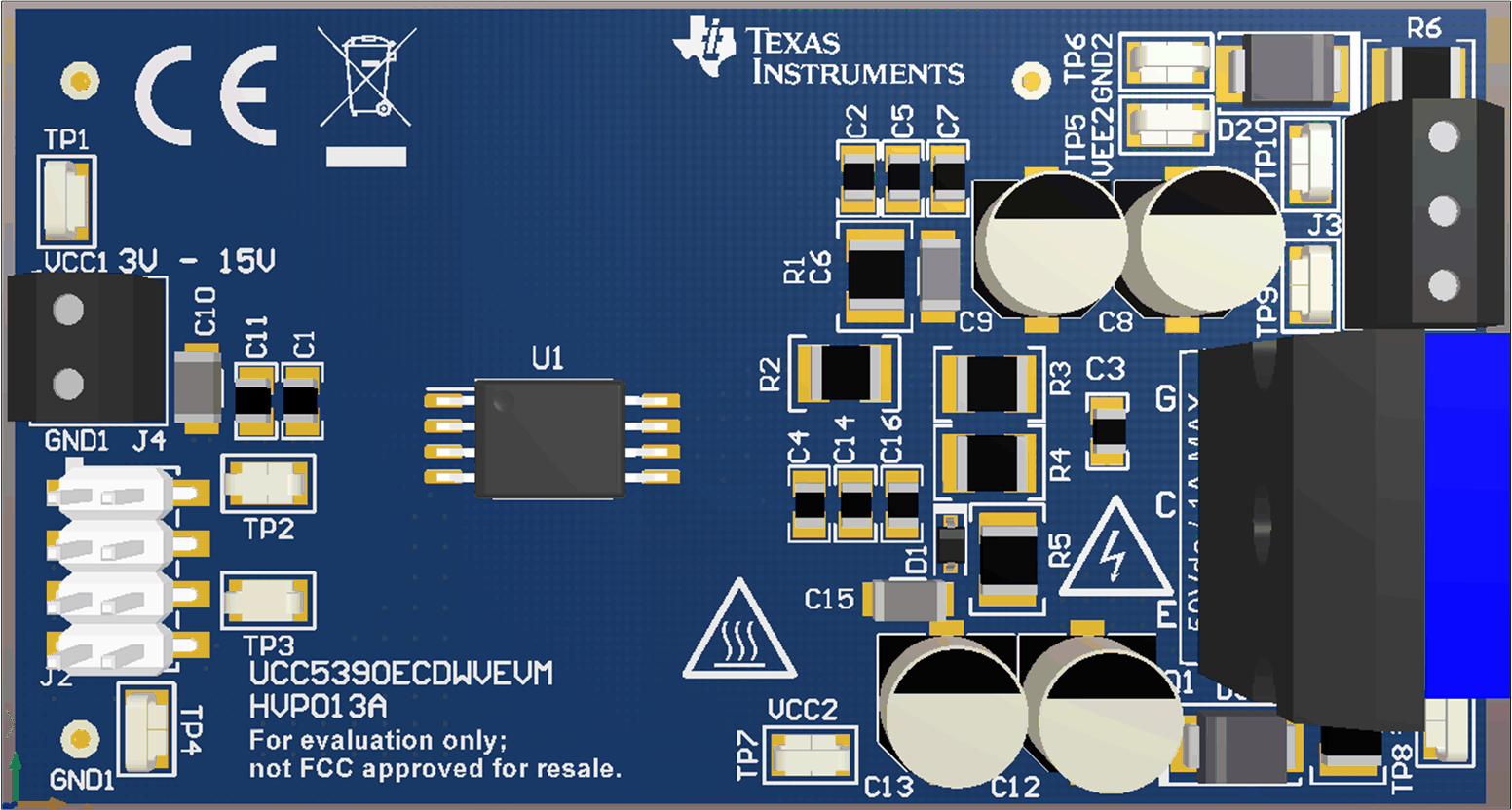
(Flipped)Figure 11-4 shows the 3D layout of the top view of the PCB.
 Figure 11-4 3-D PCB View