SLLSEI8D June 2014 – April 2015 ISO7310C , ISO7310FC
PRODUCTION DATA.
- 1 Features
- 2 Applications
- 3 Description
- 4 Revision History
- 5 Pin Configuration and Functions
- 6 Specifications
- 7 Parameter Measurement Information
- 8 Detailed Description
- 9 Applications and Implementation
- 10Power Supply Recommendations
- 11Layout
- 12Device and Documentation Support
- 13Mechanical, Packaging, and Orderable Information
パッケージ・オプション
デバイスごとのパッケージ図は、PDF版データシートをご参照ください。
メカニカル・データ(パッケージ|ピン)
- D|8
サーマルパッド・メカニカル・データ
発注情報
1 Features
- Signaling Rate: 25 Mbps
- Integrated Noise Filter at the Input
- Default Output 'High' and 'Low' Options
- Low Power Consumption: Typical ICC
- 1.9 mA at 1 Mbps, 3.8 mA at 25 Mbps (5V Supplies)
- 1.4 mA at 1 Mbps, 2.6 mA at 25 Mbps (3.3V Supplies)
- Low Propagation Delay: 32 ns Typical (5V Supplies)
- 3.3 V and 5 V Level Translation
- Wide TA Range Specified: –40°C to 125°C
- 65 KV/μs Transient Immunity, Typical (5V Supplies)
- Robust Electromagnetic Compatibility (EMC)
- System-level ESD, EFT, and Surge Immunity
- Low Emissions
- Isolation Barrier Life: > 25 Years
- Operates from 3.3 V and 5 V Supplies
- Narrow Body SOIC-8 Package
- Safety and Regulatory Approvals:
- 4242 VPK Isolation per DIN V VDE V 0884-10 and DIN EN 61010-1
- 3000 VRMS Isolation for 1 minute per UL 1577
- CSA Component Acceptance Notice 5A,
IEC 60950-1 and IEC 61010-1 End Equipment Standards - CQC Certification per GB4943.1-2011
2 Applications
- Opto-Coupler Replacement in:
- Industrial FieldBus
- ProfiBus
- ModBus
- DeviceNet™ Data Buses
- Servo Control Interface
- Motor Control
- Power Supplies
- Battery Packs
- Industrial FieldBus
3 Description
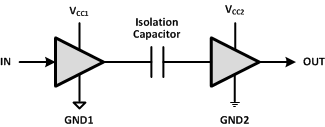
ISO7310x provide galvanic isolation up to 3000 VRMS for 1 minute per UL and 4242 VPK per VDE. These devices have one isolated channel comprised of a logic input and output buffer separated by a silicon dioxide (SiO2) insulation barrier. Used in conjunction with isolated power supplies, ISO7310x prevent noise currents on a data bus or other circuit from entering the local ground and interfering with or damaging sensitive circuitry. These devices have integrated noise filters for harsh industrial environment where short noise pulses may be present at the device input pins. ISO7310x have TTL input thresholds and operate from 3 V to 5.5 V supply levels. Through innovative chip design and layout techniques, electromagnetic compatibility of ISO7310x has been significantly enhanced to enable system-level ESD, EFT, Surge and Emissions compliance.
Device Information(1)
| PART NUMBER | PACKAGE | BODY SIZE (NOM) |
|---|---|---|
| ISO7310C | SOIC (8) | 4,90mm x 3,91mm |
| ISO7310FC |
- For all available packages, see the orderable addendum at the end of the datasheet.
4 Revision History
Changes from C Revision (March 2015) to D Revision
- Added "and DINEN 61010-1" to the 4242 VPK in the FeaturesGo
- Deleted "(Approval Pending)" from the CSA Component Acceptance list item in the FeaturesGo
- Deleted IEC from the section title: Insulation and Safety-Related Specifications for D-8 PackageGo
- Changed the CTI Test Conditions in Insulation and Safety-Related Specifications for D-8 PackageGo
- Changed VISO Test Condition in the Insulation Characteristics table Go
- Changed column CSA in the Regulatory Information tableGo
Changes from B Revision (September 2014) to C Revision
- Changed Features From: Integrated Noise Filter on the Input pin To: Integrated Noise Filter at the InputGo
- Added Features - Default Output 'High' and 'Low' OptionsGo
- Changed the DIN V VDE 0884-10 To: DIN V VDE V 0884-10 in the FeaturesGo
- Changed Features From: 3 KVRMS Isolation To: 3000 VRMS IsolationGo
- Added "(Approval Pending)" to the CSA Component Acceptance list item in the FeaturesGo
- Changed Features From: GB4943.1-2011 CQC Certification To: CQC Certification per GB4943.1-2011Go
- Changed the Simplified Schematic: GND1 To: GNDI and GND2 To GNDOGo
- Changed the Handling Ratings to ESD Ratings table and updated guidelinesGo
- Changed the CTI MIN value in Insulation and Safety-Related Specifications for D-8 PackageFrom: >400 V To: 400 VGo
- Added "DT1" to the Minimum internal gap in Insulation and Safety-Related Specifications for D-8 PackageGo
- Changed the DTI MIN value in Insulation and Safety-Related Specifications for D-8 Package From: 0.014 mm To: 13 µMGo
- Changed the RIO Test Condition in Insulation and Safety-Related Specifications for D-8 Package From: TA < 100°C To: TA = 25°CGo
- Changed the RIO Test Condition in Insulation and Safety-Related Specifications for D-8 Package From: TA ≤ max To: TA = 125°CGo
- Changed DIN V VDE 0884-10 To: DIN V VDE V 0884-10 in the Insulation CharacteristicsGo
- Added VIOSM to the Insulation Characteristics table Go
- Changed RS Test Conditions in Insulation Characteristics From: TS To: TS = 150°C Go
- Changed the Regulatory Information table, VDE Certified From: DIN V VDE 0884-10 To: DIN V VDE V 0884-10 (VDE V 0884-10):2006-12 and DIN EN 61010-1 (VDE 0411-1):2011-07Go
- Changed the Regulatory Information table, deleted (Approval Pending) statementGo
- Changed the Regulatory Information table, CQC Certified number From: CQC14001109540 To: CQC15001121656Go
- Changed title From: " IEC Safety Limiting Values" To: Safety Limiting ValuesGo
- Changed Table 2 Header information to include device number for the OUT column. Added Note 3. Go
- Changed Figure 14 to include a diode at VCC1 on the Input circuitGo
- Changed Figure 15Go
- Added Figure 16Go
Changes from A Revision (July 2014) to B Revision
- Added device ISO7310FC Go
- Changed Feature From: 4242 VPK Isolation per DIN EN 60747-5-5 (VDE 0884-5) To: 4242 VPK Isolation per DIN V VDE 0884-10Go
- Deleted "All Agencies Approvals Planned" from the Features Safety and Regulatory Approvals:Go
- Replaced Figure 10Go
- Changed DIN EN 60747-5-5 To: DIN V VDE 0884-10 in the Insulation CharacteristicsGo
- Changed DIN EN 60747-5-5 (VDE 0884-5) To: DIN V VDE 0884-10 in the Regulatory Information tableGo
- Added a NOTE in the Application Information section Go
Changes from * Revision (March 2014) to A Revision
