SNOSD01D May 2015 – October 2016 LDC1101
PRODUCTION DATA.
- 1 Features
- 2 Applications
- 3 Description
- 4 Simplified Schematic
- 5 Revision History
- 6 Pin Configuration and Functions
- 7 Specifications
-
8 Detailed Description
- 8.1 Overview
- 8.2 Functional Block Diagram
- 8.3 Feature Description
- 8.4
Device Functional Modes
- 8.4.1 Measurement Modes
- 8.4.2 RP+L Measurement Mode
- 8.4.3 High Resolution L (LHR) Measurement Mode
- 8.4.4 Reference Count Setting
- 8.4.5 L-Only Measurement Operation
- 8.4.6 Minimum Sensor Frequency and Watchdog Setting
- 8.4.7 Low Power Modes
- 8.4.8 Status Reporting
- 8.4.9 Switch Functionality and INTB Reporting
- 8.5 Programming
- 8.6
Register Maps
- 8.6.1 Individual Register Listings
- 8.6.2 Register RP_SET (address = 0x01) [reset = 0x07]
- 8.6.3 Register TC1 (address = 0x02) [reset = 0x90]
- 8.6.4 Register TC2 (address = 0x03) [reset = 0xA0]
- 8.6.5 Register DIG_CONF (address = 0x04) [reset = 0x03]
- 8.6.6 Register ALT_CONFIG (address = 0x05) [reset = 0x00]
- 8.6.7 Register RP_THRESH_HI_LSB (address = 0x06) [reset = 0x00]
- 8.6.8 Register RP_THRESH_HI_MSB (address = 0x07) [reset = 0x00]
- 8.6.9 Register RP_THRESH_LO_LSB (address = 0x08) [reset = 0x00]
- 8.6.10 Register RP_THRESH_LO_MSB (address = 0x09) [reset = 0x00]
- 8.6.11 Register INTB_MODE (address = 0x0A) [reset = 0x00]
- 8.6.12 9.Register START_CONFIG (address = 0x0B) [reset = 0x01]
- 8.6.13 Register D_CONFIG (address = 0x0C) [reset = 0x00]
- 8.6.14 Register L_THRESH_HI_LSB (address = 0x16) [reset = 0x00]
- 8.6.15 Register L_THRESH_HI_MSB (address = 0x17) [reset = 0x00]
- 8.6.16 Register L_THRESH_LO_LSB (address = 0x18) [reset = 0x00]
- 8.6.17 Register L_THRESH_LO_MSB (address = 0x19) [reset = 0x00]
- 8.6.18 Register STATUS (address = 0x020 [reset = 0x00]
- 8.6.19 Register RP_DATA_LSB (address = 0x21) [reset = 0x00]
- 8.6.20 Register RP_DATA_MSB (address = 0x22) [reset = 0x00]
- 8.6.21 Register L_DATA_LSB (address = 0x23) [reset = 0x00]
- 8.6.22 Register L_DATA_MSB (address = 0x24) [reset = 0x00]
- 8.6.23 Register LHR_RCOUNT_LSB (address = 0x30) [reset = 0x00]
- 8.6.24 Register LHR_RCOUNT_MSB (address = 0x31) [reset = 0x00]
- 8.6.25 Register LHR_OFFSET_LSB (address = 0x32) [reset = 0x00]
- 8.6.26 Register LHR_OFFSET_MSB (address = 0x33) [reset = 0x00]
- 8.6.27 Register LHR_CONFIG (address = 0x34) [reset = 0x00]
- 8.6.28 Register LHR_DATA_LSB (address = 0x38) [reset = 0x00]
- 8.6.29 Register LHR_DATA_MID (address = 0x39) [reset = 0x00]
- 8.6.30 Register LHR_DATA_MSB (address = 0x3A) [reset = 0x00]
- 8.6.31 Register LHR_STATUS (address = 0x3B) [reset = 0x00]
- 8.6.32 Register RID (address = 0x3E) [reset = 0x02]
- 8.6.33 Register DEVICE_ID (address = 0x3F) [reset = 0xD4]
-
9 Application and Implementation
- 9.1
Application Information
- 9.1.1 TI Designs and Application Notes
- 9.1.2 Theory of Operation
- 9.1.3 RP+L Mode Calculations
- 9.1.4 LDC1101 RP Configuration
- 9.1.5 Setting Internal Time Constant 1
- 9.1.6 Setting Internal Time Constant 2
- 9.1.7 MIN_FREQ and Watchdog Configuration
- 9.1.8 RP+L Sample Rate Configuration With RESP_TIME
- 9.1.9 High Resolution Inductance Calculation (LHR mode)
- 9.1.10 LHR Sample Rate Configuration With RCOUNT
- 9.1.11 Setting RPMIN for LHR Measurements
- 9.1.12 Sensor Input Divider
- 9.1.13 Reference Clock Input
- 9.1.14 INTB Reporting on SDO
- 9.1.15 DRDY (Data Ready) Reporting on SDO
- 9.1.16 Comparator Functionality
- 9.2 Typical Application
- 9.1
Application Information
- 10Power Supply Recommendations
- 11Layout
- 12Device and Documentation Support
- 13Mechanical, Packaging, and Orderable Information
パッケージ・オプション
メカニカル・データ(パッケージ|ピン)
- DRC|10
サーマルパッド・メカニカル・データ
- DRC|10
発注情報
1 Features
- Wide Operating Voltage Range: 1.8 V to 3.3 V
- Sensor Frequency Range: 500 kHz to 10 MHz
- RP Resolution: 16-Bit
- L Resolution: 16- or 24-Bit
- 180-kSPS Conversion Rate
- Threshold Detection Functionality
- 1% Part-to-Part Variation in RP Measurement
- Supply Current:
- 1.4-µA Shutdown mode
- 135-µA Sleep mode
- 1.9-mA Active Mode (no sensor connected)
- Sub-Micron Distance Resolution Achievable
- Remote Sensor Placement Isolating the LDC from Harsh Environments
- Robust Against Environmental Interferences such as Oil, Water, Dirt, or Dust
- Minimal External Components
- Magnet-Free Operation
- Operating Temperature: –40°C to +125°C
2 Applications
- High-Speed Gear Counting
- High-Speed Event Counting
- Motor Speed Sensing
- Knobs and Dials for Appliances, Automotive, and Consumer Applications
- HMI for Appliances, Automotive, and Consumer Applications
- Buttons and Keypads
- Motor Control
- Metal Detection
3 Description
The LDC1101 is a 1.8-V to 3.3-V, high-resolution inductance-to-digital converter for short-range, high-speed, contactless sensing of position, rotation, or motion, enabling reliable, accurate measurements even in the presence of dust or dirt, making it ideal for open or harsh environments.
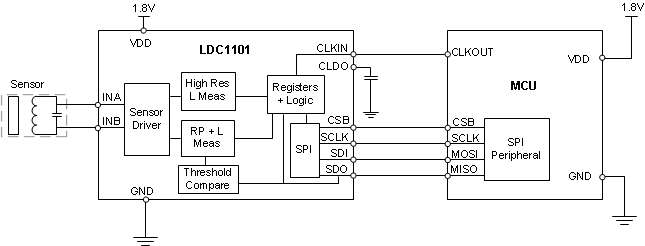
The LDC1101 features dual inductive measurement cores, allowing for > 150 ksps 16-bit RP and L measurements simultaneous with a high-resolution L measurement which can sample at > 180 ksps with a resolution of up to 24 bits. The LDC1101 includes a threshold-compare function which can be dynamically updated while the device is running.
Inductive sensing technology enables precise measurement of linear/angular position, displacement, motion, compression, vibration, metal composition, and many other applications in markets including automotive, consumer, computer, industrial, medical, and communications. Inductive sensing offers better performance and reliability at lower cost than other, competing solutions.
The LDC1101 offers these benefits of inductive sensing in a small 3-mm × 3-mm 10-pin VSON package. The LDC1101 can be easily configured by a microcontroller using the 4-pin SPI™.
Device Information(1)
| PART NUMBER | PACKAGE | BODY SIZE (NOM) |
|---|---|---|
| LDC1101 | VSON (10) | 3.00 mm × 3.00 mm |
- For all available packages, see the orderable addendum at the end of the data sheet.
4 Simplified Schematic
