SNOSCZ6 April 2016 LDC1312-Q1 , LDC1314-Q1
PRODUCTION DATA.
- 1 Features
- 2 Applications
- 3 Description
- 4 Revision History
- 5 Description Continued
- 6 Pin Configuration and Functions
- 7 Specifications
-
8 Detailed Description
- 8.1 Overview
- 8.2 Functional Block Diagram
- 8.3 Feature Description
- 8.4 Device Functional Modes
- 8.5 Programming
- 8.6
Register Maps
- 8.6.1 Register List
- 8.6.2 Address 0x00, DATA_CH0
- 8.6.3 Address 0x02, DATA_CH1
- 8.6.4 Address 0x04, DATA_CH2 (LDC1314 only)
- 8.6.5 Address 0x06, DATA_CH3 (LDC1314 only)
- 8.6.6 Address 0x08, RCOUNT_CH0
- 8.6.7 Address 0x09, RCOUNT_CH1
- 8.6.8 Address 0x0A, RCOUNT_CH2 (LDC1314 only)
- 8.6.9 Address 0x0B, RCOUNT_CH3 (LDC1314 only)
- 8.6.10 Address 0x0C, OFFSET_CH0
- 8.6.11 Address 0x0D, OFFSET_CH1
- 8.6.12 Address 0x0E, OFFSET_CH2 (LDC1314 only)
- 8.6.13 Address 0x0F, OFFSET_CH3 (LDC1314 only)
- 8.6.14 Address 0x10, SETTLECOUNT_CH0
- 8.6.15 Address 0x11, SETTLECOUNT_CH1
- 8.6.16 Address 0x12, SETTLECOUNT_CH2 (LDC1314 only)
- 8.6.17 Address 0x13, SETTLECOUNT_CH3 (LDC1314 only)
- 8.6.18 Address 0x14, CLOCK_DIVIDERS_CH0
- 8.6.19 Address 0x15, CLOCK_DIVIDERS_CH1
- 8.6.20 Address 0x16, CLOCK_DIVIDERS_CH2 (LDC1314 only)
- 8.6.21 Address 0x17, CLOCK_DIVIDERS_CH3 (LDC1314 only)
- 8.6.22 Address 0x18, STATUS
- 8.6.23 Address 0x19, ERROR_CONFIG
- 8.6.24 Address 0x1A, CONFIG
- 8.6.25 Address 0x1B, MUX_CONFIG
- 8.6.26 Address 0x1C, RESET_DEV
- 8.6.27 Address 0x1E, DRIVE_CURRENT_CH0
- 8.6.28 Address 0x1F, DRIVE_CURRENT_CH1
- 8.6.29 Address 0x20, DRIVE_CURRENT_CH2 (LDC1314 only)
- 8.6.30 Address 0x21, DRIVE_CURRENT_CH3 (LDC1314 only)
- 8.6.31 Address 0x7E, MANUFACTURER_ID
- 8.6.32 Address 0x7F, DEVICE_ID
- 9 Application and Implementation
- 10Power Supply Recommendations
- 11Layout
- 12Device and Documentation Support
- 13Mechanical, Packaging, and Orderable Information
パッケージ・オプション
メカニカル・データ(パッケージ|ピン)
- RGH|16
サーマルパッド・メカニカル・データ
- RGH|16
発注情報
1 Features
- Qualified for Automotive Applications
- AEC-Q100 Qualified With the Following Results:
- Device Temperature Grade 1:–40°C to +125°C Ambient Operating Temperature Range
- Device HBM ESD Classification Level 2
- Device CDM ESD Classification Level C5
- Easy-to-use – Minimal Configuration Required
- Measure up to 4 Sensors with One IC
- Multiple Channels Support Environmental and Aging Compensation
- Multi-Channel Remote Sensing Provides Lowest System Cost
- Pin-Compatible Medium and High-resolution Options
- LDC1312-Q1/LDC1314-Q1: 2/4-ch 12-bit LDC
- LDC1612-Q1/LDC1614-Q1: 2/4-ch 28-bit LDC
- Supports Wide Sensor Frequency Range of 1kHz to 10MHz
- Power Consumption:
- 35 µA Low Power Sleep Mode
- 200 nA Shutdown Mode
- 3.3V Operation
- Support Internal or External Reference Clock
- Immune to DC Magnetic Fields and Magnets
2 Applications
- Automotive Buttons and Knobs
- Linear and Rotational Encoders
- Slider Buttons
- Metal Detection in Industrial and Automotive
- Flow Meters
3 Description
The LDC1312-Q1 and LDC1314-Q1 are 2- and 4-channel, 12-bit inductance to digital converters (LDCs) for inductive sensing solutions. With multiple channels and support for remote sensing, the LDC1312-Q1 and LDC1314-Q1 enable the performance and reliability benefits of inductive sensing to be realized at minimal cost and power. The products are easy to use, only requiring that the sensor frequency be within 1 kHz and 10 MHz to begin sensing. The wide 1 kHz to 10 MHz sensor frequency range also enables use of very small PCB coils, further reducing sensing solution cost and size.
Device Information(1)
| PART NUMBER | PACKAGE | BODY SIZE (NOM) |
|---|---|---|
| LDC1312-Q1 | WSON (12) | 4.00 mm × 4.00 mm |
| LDC1314-Q1 | WQFN (16) | 4.00 mm × 4.00 mm |
- For all available packages, see the orderable addendum at the end of the data sheet.
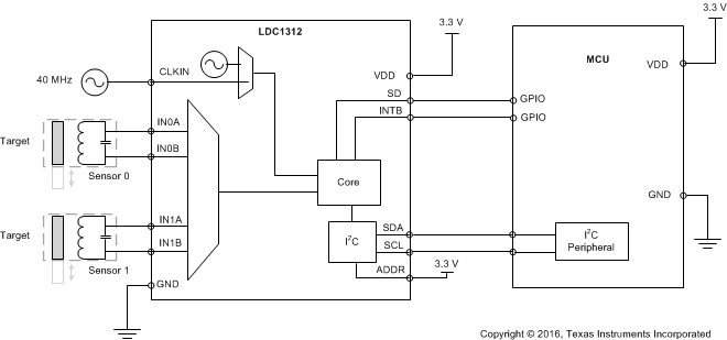
Simplified Schematic

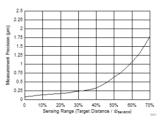
Measurement Precision vs. Target Distance
