JAJSCO0D November 2016 – August 2021 LM5170-Q1
PRODUCTION DATA
- 1 特長
- 2 アプリケーション
- 3 概要
- 4 Revision History
- 5 概要 (続き)
- 6 Pin Configuration and Functions
- 7 Specifications
-
8 Detailed Description
- 8.1 Overview
- 8.2 Functional Block Diagram
- 8.3
Feature Description
- 8.3.1 Bias Supply (VCC, VCCA)
- 8.3.2 Undervoltage Lockout (UVLO) and Master Enable or Disable
- 8.3.3 High Voltage Input (VIN, VINX)
- 8.3.4 Current Sense Amplifier
- 8.3.5 Control Commands
- 8.3.6 Channel Current Monitor (IOUT1, IOUT2)
- 8.3.7 Cycle-by-Cycle Peak Current Limit (IPK)
- 8.3.8 Error Amplifier
- 8.3.9 Ramp Generator
- 8.3.10 Soft Start
- 8.3.11 Gate Drive Outputs, Dead Time Programming and Adaptive Dead Time (HO1, HO2, LO1, LO2, DT)
- 8.3.12 PWM Comparator
- 8.3.13 Oscillator (OSC)
- 8.3.14 Synchronization to an External Clock (SYNCIN, SYNCOUT)
- 8.3.15 Diode Emulation
- 8.3.16 Power MOSFET Failure Detection and Failure Protection (nFAULT, BRKG, BRKS)
- 8.3.17 Overvoltage Protection (OVPA, OVPB)
- 8.4 Device Functional Modes
- 8.5 Programming
-
9 Application and Implementation
- 9.1 Application Information
- 9.2
Typical Application
- 9.2.1
60-A, Dual-Phase, 48-V to 12-V Bidirectional Converter
- 9.2.1.1 Design Requirements
- 9.2.1.2
Detailed Design Procedure
- 9.2.1.2.1 Determining the Duty Cycle
- 9.2.1.2.2 Oscillator Programming
- 9.2.1.2.3 Power Inductor, RMS and Peak Currents
- 9.2.1.2.4 Current Sense (RCS)
- 9.2.1.2.5 Current Setting Limits (ISETA or ISETD)
- 9.2.1.2.6 Peak Current Limit
- 9.2.1.2.7 Power MOSFETS
- 9.2.1.2.8 Bias Supply
- 9.2.1.2.9 Boot Strap
- 9.2.1.2.10 RAMP Generators
- 9.2.1.2.11 OVP
- 9.2.1.2.12 Dead Time
- 9.2.1.2.13 IOUT Monitors
- 9.2.1.2.14 UVLO Pin Usage
- 9.2.1.2.15 VIN Pin Configuration
- 9.2.1.2.16 Loop Compensation
- 9.2.1.2.17 Soft Start
- 9.2.1.2.18 ISET Pins
- 9.2.1.3 Application Curves
- 9.2.1
60-A, Dual-Phase, 48-V to 12-V Bidirectional Converter
- 10Power Supply Recommendations
- 11Layout
- 12Device and Documentation Support
- 13Mechanical, Packaging, and Orderable Information
9.2.1.2.7 Power MOSFETS
The power MOSFETs must be chosen with a VDS rating capable of withstanding the maximum HV-port voltage plus transient spikes (ringing). In this example, the maximum HV-rail voltage is 70 V. Selecting the 80 V rated MOSFETs will allow 10-V transient spikes.
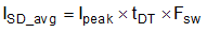
When the voltage rating is determined, select the MOSFETs by making tradeoffs between the MOSFET Rds(ON) and total gate charge Qg to balance the conduction and switching losses. For high power applications, parallel MOSFETs to share total power and reduce the dissipation on any individual MOSFET, hence relieving the thermal stress. The conduction losses in each MOSFET is determined by Equation 53.
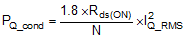
where
- N is the number of MOSFETs in parallel
- 1.8 is the approximate temperature coefficient of the Rds(ON) at 125 °C
- and the total RMS switch current IQ_RMS is approximately determined by Equation 54

where
- Dmax is the maximum duty cycle, either in the buck mode or boost mode.
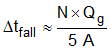
The switching transient rise and fall times are approximately determined by:

And the switching losses of each of the paralleled MOSFETs are approximately determined by:
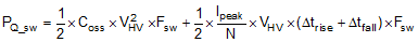
where
- Coss is the MOSFET’s output capacitance.
The power MOSFET usually requires a gate-to-source resistor of 10 kΩ to 100 kΩ to mitigate the effects of a failed gate drive. When using parallel MOSFETs, a good practice is to use 1- to 2-Ω gate resistor for each MOSFET, as shown in Figure 9-10.
 Figure 9-10 Paralleled MOSFET Configuration
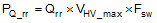
If the dead time is not optimal, the body diode of the power synchronous rectifier MOSFET will cause losses in reverse recovery. Assuming the reverse recovery charge of the power MOSFET is Qrr, the reverse recovery losses are thus determined by Equation 58:
To reduce the reverse recovery losses, an optional Schottky diode can be placed in parallel with the power MOSFETs. The diode should have the same voltage rating as the MOSFET, and it must be placed directly across the MOSFETs drain and source. The peak repetitive forward current rating should be greater than Ipeak, and the continuous forward current rating should be greater than the following Equation 59: