JAJSGI4B November 2018 – March 2021 ADC12DJ3200QML-SP
PRODUCTION DATA
- 1 特長
- 2 アプリケーション
- 3 概要
- 4 Revision History
- 5 Pin Configuration and Functions
-
6 Specifications
- 6.1 Absolute Maximum Ratings
- 6.2 ESD Ratings
- 6.3 Recommended Operating Conditions
- 6.4 Thermal Information
- 6.5 Electrical Characteristics: DC Specifications
- 6.6 Electrical Characteristics: Power Consumption
- 6.7 Electrical Characteristics: AC Specifications (Dual-Channel Mode)
- 6.8 Electrical Characteristics: AC Specifications (Single-Channel Mode)
- 6.9 Timing Requirements
- 6.10 Switching Characteristics
- 6.11 Timing Diagrams
- 6.12 Typical Characteristics
-
7 Detailed Description
- 7.1 Overview
- 7.2 Functional Block Diagram
- 7.3
Feature Description
- 7.3.1 Analog Inputs
- 7.3.2 ADC Core
- 7.3.3 Timestamp
- 7.3.4 Clocking
- 7.3.5 Digital Down Converters (Dual-Channel Mode Only)
- 7.3.6 JESD204B Interface
- 7.3.7 Alarm Monitoring
- 7.3.8 Temperature Monitoring Diode
- 7.3.9 Analog Reference Voltage
- 7.4
Device Functional Modes
- 7.4.1 Dual-Channel Mode
- 7.4.2 Single-Channel Mode (DES Mode)
- 7.4.3 JESD204B Modes
- 7.4.4 Power-Down Modes
- 7.4.5 Test Modes
- 7.4.6 Calibration Modes and Trimming
- 7.4.7 Offset Calibration
- 7.4.8 Trimming
- 7.4.9 Offset Filtering
- 7.5 Programming
- 7.6 Register Maps
- 8 Application Information Disclaimer
- 9 Layout
- 10Device and Documentation Support
7.3.5.2 Decimation Filters
The decimation filters are arranged to provide a programmable overall decimation of 2, 4, 8, or 16. All filter outputs have a resolution of 15 bits. The decimate-by-2 filter has a real output and the decimate-by-4, decimate-by-8, and decimate-by-16 filters have complex outputs. Table 7-10 lists the effective output sample rates, available signal bandwidths, output formats, and stop-band attenuation for each decimation mode. The available bandwidths of the complex output modes are twice that of equivalent real decimation modes because of the nature of the I/Q data and complex signaling. This higher bandwidth results in the decimate-by-2 real and decimate-by-4 complex modes having approximately the same useful output bandwidth.
| DECIMATION SETTING | ƒ(DEVCLK) | OUTPUT FORMAT | |||
|---|---|---|---|---|---|
| OUTPUT RATE (MSPS) | MAX ALIAS PROTECTED SIGNAL BANDWIDTH (MHz) | STOP-BAND ATTENUATION | PASS-BAND RIPPLE | ||
| No decimation | ƒ(DEVCLK) | ƒ(DEVCLK) / 2 | — | < ±0.001 dB | Real signal, 12-bit data |
| Decimate-by-2 | ƒ(DEVCLK) / 2 | 0.4 × ƒ(DEVCLK) / 2 | > 89 dB | < ±0.001 dB | Real signal, 15-bit data |
| Decimate-by-4 (D4_AP87 = 0) | ƒ(DEVCLK) / 4 | 0.8 × ƒ(DEVCLK) / 4 | > 90 dB | < ±0.001 dB | Complex signal, 15-bit data |
| Decimate-by-4 (D4_AP87 = 1) | ƒ(DEVCLK) / 4 | 0.875 × ƒ(DEVCLK) / 4 | > 66 dB | < ±0.005 dB | Complex signal, 15-bit data |
| Decimate-by-8 | ƒ(DEVCLK) / 8 | 0.8 × ƒ(DEVCLK) / 8 | > 90 dB | < ±0.001 dB | Complex signal, 15-bit data |
| Decimate-by-16 | ƒ(DEVCLK) / 16 | 0.8 × ƒ(DEVCLK) / 16 | > 90 dB | < ±0.001 dB | Complex signal, 15-bit data |
Figure 7-7 to Figure 7-18 provide the composite decimation filter responses. The pass-band section (black trace) shows the alias-protected region of the response. The transition band (red trace) shows the transition region of the response, or the regions that alias into the transition region, which is not alias protected and therefore desired signals must not be within this band. The aliasing band (blue trace) shows the attenuation applied to the bands that alias back into the pass band after decimation and are sufficiently low to prevent undesired signals from showing up in the pass band. Use analog input filtering for additional attenuation of the aliasing band or to prevent harmonics, interleaving spurs, or other undesired spurious signals from folding into the desired signal band before the decimation filter.
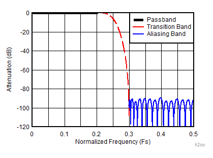
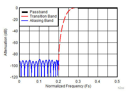
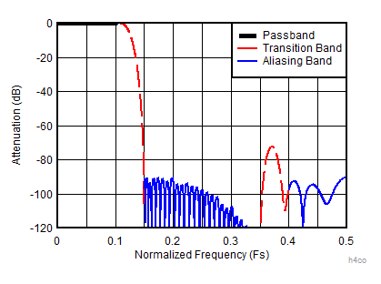
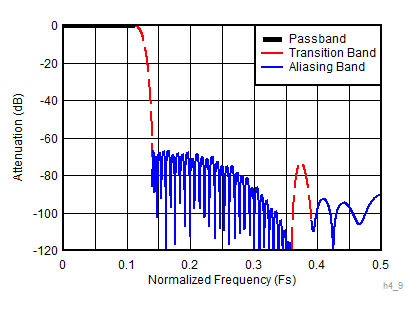
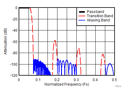
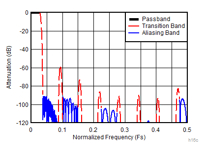
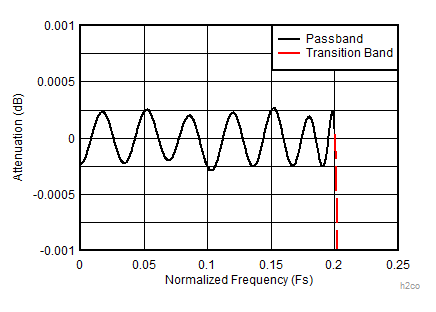
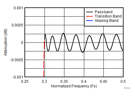
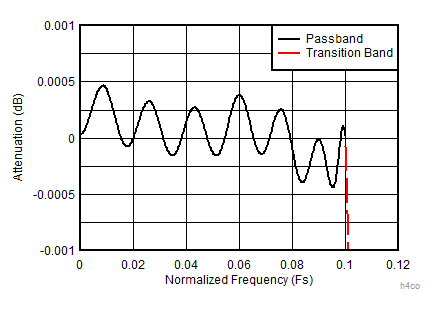
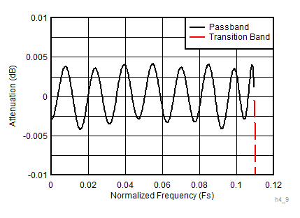
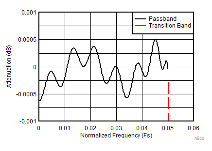
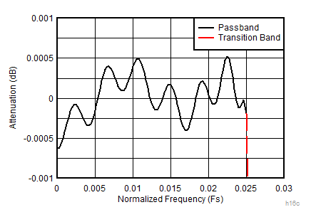
For maximum efficiency, a group of high-speed filter blocks are implemented with specific blocks used for each decimation setting to achieve the composite responses illustrated in Figure 7-7 to Figure 7-18. Table 7-11 describes the combination of filter blocks used for each decimation setting and Table 7-12 lists the coefficient details and decimation factor of each filter block. The coefficients are symmetric with the center tap indicated by bold text.
| DECIMATION SETTING | FILTER BLOCKS USED |
|---|---|
| 2 | CS80 |
| 4 (D4_AP87 = 0) | CS45, CS80 |
| 4 (D4_AP87 = 1) | CS45, CS87 |
| 8 | CS20, CS40, CS80 |
| 16 | CS10, CS20, CS40, CS80 |
| FILTER COEFFICIENT SET (Decimation Factor of Filter) | |||||||||||
|---|---|---|---|---|---|---|---|---|---|---|---|
| CS10 (2) | CS20 (2) | CS40 (2) | CS45 (2) | CS80 (2) | CS87 (2) | ||||||
| –65 | –65 | 109 | 109 | –327 | –327 | 56 | 56 | –37 | –37 | –15 | –15 |
| 0 | 0 | 0 | 0 | 0 | 0 | 0 | 0 | 0 | 0 | 0 | 0 |
| 577 | 577 | –837 | –837 | 2231 | 2231 | –401 | –401 | 118 | 118 | 23 | 23 |
| 1024 | 0 | 0 | 0 | 0 | 0 | 0 | 0 | 0 | 0 | 0 | |
| 4824 | 4824 | –8881 | –8881 | 1596 | 1596 | –291 | –291 | –40 | –40 | ||
| 8192 | 0 | 0 | 0 | 0 | 0 | 0 | 0 | 0 | |||
| 39742 | 39742 | –4979 | –4979 | 612 | 612 | 64 | 64 | ||||
| 65536 | 0 | 0 | 0 | 0 | 0 | 0 | |||||
| 20113 | 20113 | –1159 | –1159 | –97 | –97 | ||||||
| 32768 | 0 | 0 | 0 | 0 | |||||||
| 2031 | 2031 | 142 | 142 | ||||||||
| 0 | 0 | 0 | 0 | ||||||||
| –3356 | –3356 | –201 | –201 | ||||||||
| 0 | 0 | 0 | 0 | ||||||||
| 5308 | 5308 | 279 | 279 | ||||||||
| 0 | 0 | 0 | 0 | ||||||||
| –8140 | –8140 | –380 | –380 | ||||||||
| 0 | 0 | 0 | 0 | ||||||||
| 12284 | 12284 | 513 | 513 | ||||||||
| 0 | 0 | 0 | 0 | ||||||||
| –18628 | –18628 | –690 | –690 | ||||||||
| 0 | 0 | 0 | 0 | ||||||||
| 29455 | 29455 | 939 | 939 | ||||||||
| 0 | 0 | 0 | 0 | ||||||||
| –53191 | –53191 | –1313 | –1313 | ||||||||
| 0 | 0 | 0 | 0 | ||||||||
| 166059 | 166059 | 1956 | 1956 | ||||||||
| 262144 | 0 | 0 | |||||||||
| –3398 | –3398 | ||||||||||
| 0 | 0 | ||||||||||
| 10404 | 10404 | ||||||||||
| 16384 | |||||||||||