JAJU648A November   2018  – April 2022 TLV3601 , TLV3601-Q1 , TLV3603 , TLV3603-Q1


  1.   概要
  2.   Resources
  3.   特長
  4.   アプリケーション
  5.   5
  6. 1System Description
    1. 1.1 Key System Specifications
  7. 2System Overview
    1. 2.1 Block Diagram
    2. 2.2 Design Considerations
      1. 2.2.1 Amplifier and Comparator
      2. 2.2.2 Digital Processing and Control
      3. 2.2.3 Optical Components
        1. 2.2.3.1 Laser Driver and Laser Diode
        2. 2.2.3.2 Photodiode
      4. 2.2.4 Power Supply
    3. 2.3 Highlighted Products
      1. 2.3.1 OPA858 Operational Amplifier
      2. 2.3.2 TLV3501 and TLV3601/3 High-Speed Comparators
      3. 2.3.3 TDC7201 Time-to-Digital Converter
    4. 2.4 System Design Theory
      1. 2.4.1 Transimpedance Amplifier
        1. 2.4.1.1 Bandwidth
        2. 2.4.1.2 Stability Considerations
        3. 2.4.1.3 Noise Performance
      2. 2.4.2 Time-of-Flight Measurement
      3. 2.4.3 Simulations
        1. 2.4.3.1 Bandwidth Simulation
        2. 2.4.3.2 Noise Simulation
        3. 2.4.3.3 OPA858 Loop-Gain and Phase Margin Simulation
  8. 3Hardware, Software, Testing Requirements, and Test Results
    1. 3.1 Required Hardware and Software
      1. 3.1.1 Hardware
      2. 3.1.2 Software
    2. 3.2 Testing and Results
      1. 3.2.1 Test Setup
        1. 3.2.1.1 Getting Started: System Setup
          1. 3.2.1.1.1 Laser-Driver Setup
          2. 3.2.1.1.2 Receiver and Optical Setup
      2. 3.2.2 Test Results
        1. 3.2.2.1 Verification and Measured Performance
          1. 3.2.2.1.1 Pulse Response Measurements
            1. 3.2.2.1.1.1 Pulse Response Settling
            2. 3.2.2.1.1.2 Pulse Response vs Output Pulse Width
            3. 3.2.2.1.1.3 Rise and Fall Time
            4. 3.2.2.1.1.4 Overdriven Response
          2. 3.2.2.1.2 Time-of-Flight Test
          3. 3.2.2.1.3 Time-of-Flight Measurement Error Sources
  9. 4Design Files
    1. 4.1 Schematics
    2. 4.2 Bill of Materials
    3. 4.3 PCB Layout Recommendations
      1. 4.3.1 Layout Prints
    4. 4.4 Altium Project
    5. 4.5 Gerber Files
  10. 5Related Documentation
    1. 5.1 Trademarks
  11. 6About the Author
  12. 7Revision History

OPA858 Operational Amplifier

The OPA858 is a wideband, low-noise, operational amplifier with CMOS inputs for wideband transimpedance and voltage amplifier applications. When the device is configured as a transimpedance amplifier (TIA), the 5.5-GHz gain bandwidth product (GBP) enables applications requiring high closed-loop bandwidths at transimpedance gains in the tens to hundreds of kilohms range.

Figure 2-3 and Figure 2-4 demonstrate the bandwidth and noise performance of the OPA858 as a function of the photodiode capacitance when the amplifier is configured as a TIA. The total noise is calculated over a bandwidth range extending from DC to the calculated f–3dB frequency on the left-hand scale. The OPA858 package features a feedback pin (FB) that simplifies the feedback network connection between the input and the output.
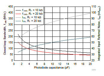
GUID-15CF6ED1-8179-4F73-B198-2048AC8C6D84-low.gifFigure 2-3 OPA858 Bandwidth and Noise Performance vs Photodiode Capacitance
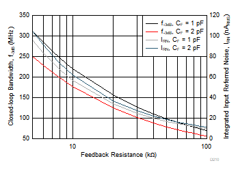
GUID-0DDC3EEF-0562-4E7F-BF3D-26D438EBE999-low.gifFigure 2-4 OPA858 Bandwidth and Noise Performance vs Feedback Resistance