JAJU648A November   2018  – April 2022 TLV3601 , TLV3601-Q1 , TLV3603 , TLV3603-Q1


  1.   概要
  2.   Resources
  3.   特長
  4.   アプリケーション
  5.   5
  6. 1System Description
    1. 1.1 Key System Specifications
  7. 2System Overview
    1. 2.1 Block Diagram
    2. 2.2 Design Considerations
      1. 2.2.1 Amplifier and Comparator
      2. 2.2.2 Digital Processing and Control
      3. 2.2.3 Optical Components
        1. 2.2.3.1 Laser Driver and Laser Diode
        2. 2.2.3.2 Photodiode
      4. 2.2.4 Power Supply
    3. 2.3 Highlighted Products
      1. 2.3.1 OPA858 Operational Amplifier
      2. 2.3.2 TLV3501 and TLV3601/3 High-Speed Comparators
      3. 2.3.3 TDC7201 Time-to-Digital Converter
    4. 2.4 System Design Theory
      1. 2.4.1 Transimpedance Amplifier
        1. 2.4.1.1 Bandwidth
        2. 2.4.1.2 Stability Considerations
        3. 2.4.1.3 Noise Performance
      2. 2.4.2 Time-of-Flight Measurement
      3. 2.4.3 Simulations
        1. 2.4.3.1 Bandwidth Simulation
        2. 2.4.3.2 Noise Simulation
        3. 2.4.3.3 OPA858 Loop-Gain and Phase Margin Simulation
  8. 3Hardware, Software, Testing Requirements, and Test Results
    1. 3.1 Required Hardware and Software
      1. 3.1.1 Hardware
      2. 3.1.2 Software
    2. 3.2 Testing and Results
      1. 3.2.1 Test Setup
        1. 3.2.1.1 Getting Started: System Setup
          1. 3.2.1.1.1 Laser-Driver Setup
          2. 3.2.1.1.2 Receiver and Optical Setup
      2. 3.2.2 Test Results
        1. 3.2.2.1 Verification and Measured Performance
          1. 3.2.2.1.1 Pulse Response Measurements
            1. 3.2.2.1.1.1 Pulse Response Settling
            2. 3.2.2.1.1.2 Pulse Response vs Output Pulse Width
            3. 3.2.2.1.1.3 Rise and Fall Time
            4. 3.2.2.1.1.4 Overdriven Response
          2. 3.2.2.1.2 Time-of-Flight Test
          3. 3.2.2.1.3 Time-of-Flight Measurement Error Sources
  9. 4Design Files
    1. 4.1 Schematics
    2. 4.2 Bill of Materials
    3. 4.3 PCB Layout Recommendations
      1. 4.3.1 Layout Prints
    4. 4.4 Altium Project
    5. 4.5 Gerber Files
  10. 5Related Documentation
    1. 5.1 Trademarks
  11. 6About the Author
  12. 7Revision History
Pulse Response Settling

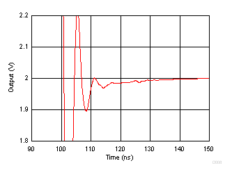
Figure 3-2 shows the standard pulse response as triggered by the MSP430. The optical power to the photodiode is controlled with an attenuator to obtain a 1.7-V output voltage amplitude. Figure 3-3 shows the detail of the pulse response settling to a final value of 2 V. Settling performance can be improved for this design by altering the amplifier response, but is not a necessity for the TDC7201-based design.
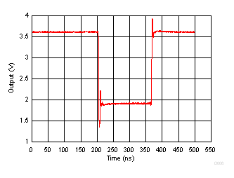
GUID-8F7D4F8C-641A-42AB-AB8B-67FC7B0E8F38-low.gifFigure 3-2 Pulse Response, 1.7-V Output
GUID-0DBFD478-7C47-47D1-BB79-3DBAC076178E-low.gifFigure 3-3 Pulse Response Settling Zoom