JAJU648A November   2018  – April 2022 TLV3601 , TLV3601-Q1 , TLV3603 , TLV3603-Q1


  1.   概要
  2.   Resources
  3.   特長
  4.   アプリケーション
  5.   5
  6. 1System Description
    1. 1.1 Key System Specifications
  7. 2System Overview
    1. 2.1 Block Diagram
    2. 2.2 Design Considerations
      1. 2.2.1 Amplifier and Comparator
      2. 2.2.2 Digital Processing and Control
      3. 2.2.3 Optical Components
        1. 2.2.3.1 Laser Driver and Laser Diode
        2. 2.2.3.2 Photodiode
      4. 2.2.4 Power Supply
    3. 2.3 Highlighted Products
      1. 2.3.1 OPA858 Operational Amplifier
      2. 2.3.2 TLV3501 and TLV3601/3 High-Speed Comparators
      3. 2.3.3 TDC7201 Time-to-Digital Converter
    4. 2.4 System Design Theory
      1. 2.4.1 Transimpedance Amplifier
        1. 2.4.1.1 Bandwidth
        2. 2.4.1.2 Stability Considerations
        3. 2.4.1.3 Noise Performance
      2. 2.4.2 Time-of-Flight Measurement
      3. 2.4.3 Simulations
        1. 2.4.3.1 Bandwidth Simulation
        2. 2.4.3.2 Noise Simulation
        3. 2.4.3.3 OPA858 Loop-Gain and Phase Margin Simulation
  8. 3Hardware, Software, Testing Requirements, and Test Results
    1. 3.1 Required Hardware and Software
      1. 3.1.1 Hardware
      2. 3.1.2 Software
    2. 3.2 Testing and Results
      1. 3.2.1 Test Setup
        1. 3.2.1.1 Getting Started: System Setup
          1. 3.2.1.1.1 Laser-Driver Setup
          2. 3.2.1.1.2 Receiver and Optical Setup
      2. 3.2.2 Test Results
        1. 3.2.2.1 Verification and Measured Performance
          1. 3.2.2.1.1 Pulse Response Measurements
            1. 3.2.2.1.1.1 Pulse Response Settling
            2. 3.2.2.1.1.2 Pulse Response vs Output Pulse Width
            3. 3.2.2.1.1.3 Rise and Fall Time
            4. 3.2.2.1.1.4 Overdriven Response
          2. 3.2.2.1.2 Time-of-Flight Test
          3. 3.2.2.1.3 Time-of-Flight Measurement Error Sources
  9. 4Design Files
    1. 4.1 Schematics
    2. 4.2 Bill of Materials
    3. 4.3 PCB Layout Recommendations
      1. 4.3.1 Layout Prints
    4. 4.4 Altium Project
    5. 4.5 Gerber Files
  10. 5Related Documentation
    1. 5.1 Trademarks
  11. 6About the Author
  12. 7Revision History

OPA858 Loop-Gain and Phase Margin Simulation

To get a pulse-response with fast rise and fall time, some overshoot and ringing on the rising and falling edges of the pulse is expected. The phase-margin of the OPA858 circuit is targeted at 55° to achieve a Q factor of 0.95. Use the circuit in Figure 2-10 to simulate the loop-gain of the OPA858. For more information on transimpedance amplifier stability theory and design, see the What You Need To Know About Transimpedance Amplifiers blog, part 1 and part 2.
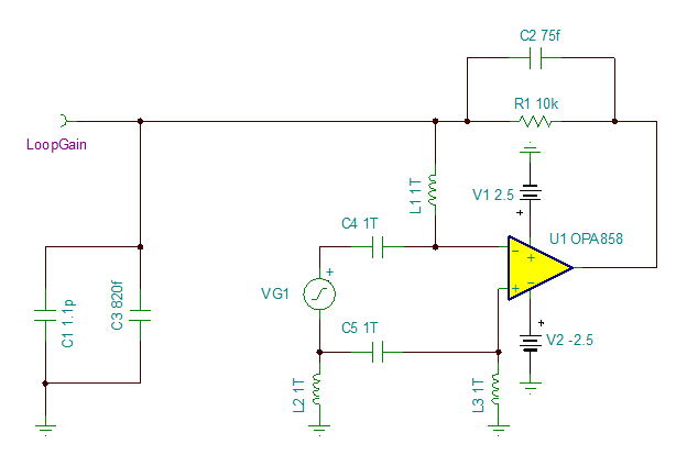
GUID-3A80B59B-9E37-4E50-8FCD-31014F5B6168-low.gifFigure 2-10 OPA858 Loop-Gain Analysis TINA Schematic

The simulated loop-gain magnitude and phase plotted in Figure 2-11 predict a phase-margin of approximately 45°, which is lower than the expected calculated value because the calculation is only a first-order approximation.
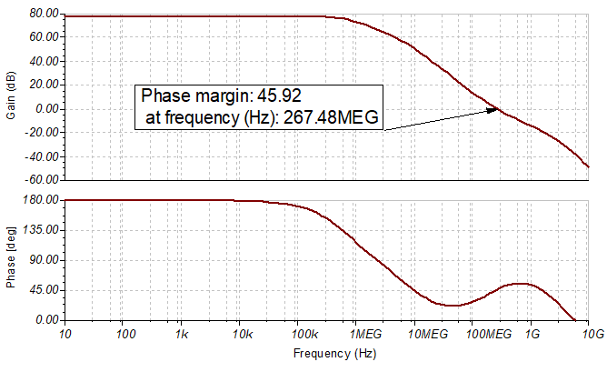
GUID-10D322B5-533D-4F13-B7F4-FBCB09145E85-low.gifFigure 2-11 Simulated Loop Gain of the OPA858 Circuit