SBAA461 December 2020 ADC3541 , ADC3542 , ADC3543 , ADC3544 , ADC3641 , ADC3642 , ADC3643 , ADC3644 , ADC3660 , ADC3681 , ADC3682 , ADC3683
2.1.1 Parallel SDR
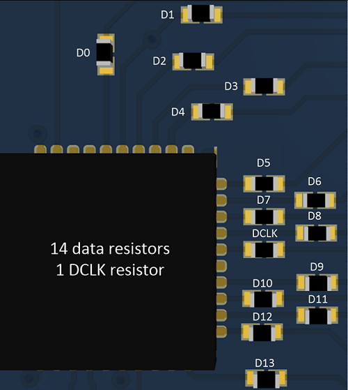
In SDR mode, each data bit corresponds to one CMOS output pin on the ADC. For a 14-bit ADC, there will be 14 resistors at each output pin, and one resistor for the data clock (DCLK) for a total of 15 pins and or resistors.
 Figure 2-1 Parallel CMOS: 14 bit SDR
Resistors
Figure 2-1 Parallel CMOS: 14 bit SDR
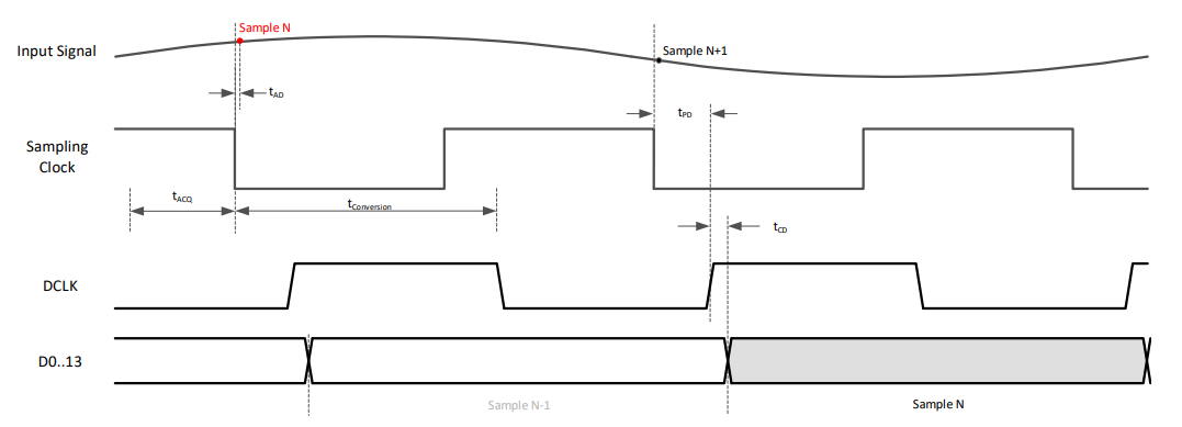
ResistorsAlso, the DCLK will latch the data on only the rising edge of the DCLK. This means that the data bits and the data clock are toggling at the same rate. For example, if the ADC3541 is sampling at 10 MSPS, the data bits and DCLK are toggling at a frequency of 10 MHz. This is actually the lowest data rate we can achieve without utilizing the on-chip digital decimation features 0f the ADC3541.
| Parallel Interface | Max Sampling Rate (MSPS) | Data Rate (Mbps) | Data Pins/Resistors |
|---|---|---|---|
| SDR | 65 | 65 | 15 |
 Figure 2-2 Parallel CMOS SDR Timing
Diagram