SBAA528 February 2022 ADC12QJ1600-Q1 , TPS62912 , TPS62913
1.1.2 Power Supply Requirements for Clocks
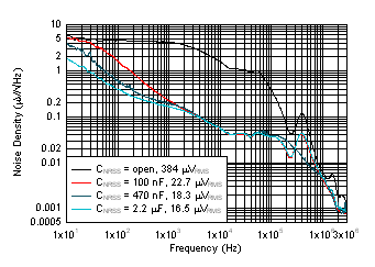
On the ADC12QJ1600-Q1 evaluation module, an external clock is provided to an ultra low noise PLL which is used for clocking the ADC. Similar to high speed ADCs, higher frequencies command larger supply currents. At the same time, higher frequencies require lower clock jitter and therefore lower phase noise. Phase noise is directly impacted by the power supply noise and ripple. The performance of the TPS62913 is shown in Figure 1-3.
 Figure 1-3 TPS62913 Output Noise Density
vs Frequency for 12Vin to 3.3Vout at 2.2 MHz
Figure 1-3 TPS62913 Output Noise Density
vs Frequency for 12Vin to 3.3Vout at 2.2 MHzThe TPS62913 has been designed specifically for low noise with the addition of an external noise reduction filter cap, which also provides the means to adjust the softstart time. Using a 470 nF CNR/SS cap provide the noise performance desired and a 5 ms softstart time.