SBAA551 June 2022 ADS8661 , ADS8665 , ADS8671 , ADS8675 , ADS8681 , ADS8685 , ADS8689 , ADS8691 , ADS8695 , ADS8699 , INA823 , INA826 , LM317L , LM337L , MUX509 , TPS2661 , TPS560430
2.1 Input Stage
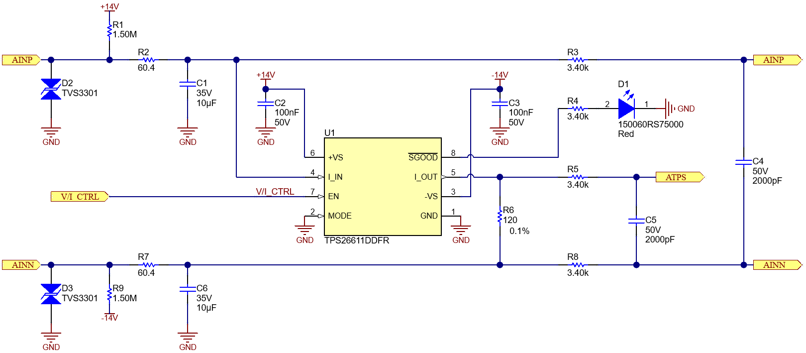
The input stage circuit protects against mis-wiring and surges. The following schematic shows the input stage for a single channel.
 Figure 2-1 V/I Switch and Filter
The input stage tolerates up to ±33 V (permanent) at the terminals in both current and voltage mode. The input protection circuit also limits the input current to ±30 mA (maximum) in current mode only and suppresses surges of ±1 kV at 42 Ω in accordance to IEC61000-4-5 specifications using the TVS3301, a 33-V bidirectional flat-clamp surge protection device. Current or voltage inputs are selected by a 3.3-V digital control signal (V/I CTRL in Figure 2-1), which controls the switch inside the TPS26611 loop protector. In voltage mode, the TPS26611 switch is open and the input signal is directly fed to the next stage. In current mode, the TPS26611 switch is closed and connects both terminal pins through the shunt resistor. The voltage drop across the shunt is the sensor signal to be measured. For high-accuracy measurements, the TPS26611 switch must be excluded and an additional signal (ATPS in Figure 2-1) is introduced. Diode D1 is the indicator of overvoltage or overcurrent condition in current mode.
Open-wire detection (OWD) is implemented by pullup and pull-down resistors at the terminals. In voltage mode, the differential input voltage clips to the rails, which results in an invalid input signal. In current mode, OWD is detected by a 0-mA reading.
Simple passives result in low-pass common-mode and differential anti-aliasing filters (AAF) that limit the input signal bandwidth and thereby reducing noise. This design supports various configurable differential filter per use-case or design need. Figure 2-1 shows common-mode filters R2, C1 and R7, C6, which each have a 256-Hz cutoff frequency. The differential filter is implemented separately for voltage and current inputs, using R3, R8, C4 and R5, R8, C5, respectively. Each differential filter has a cutoff frequency of about 12 kHz for best common-mode rejection performance of the instrumentation amplifier INA826. The AAF resistors also protect the multiplexer from excessive current in mis-wiring and surge events.