SBAU351 April   2021


  1.   Trademarks
  2. 1EVM Overview
    1. 1.1 ADS127L11EVM Kit
    2. 1.2 ADS127L11EVM Board
    3. 1.3 ADS127L11EVM-PDK-GUI Unsupported Features
  3. 2EVM Analog Interface
    1. 2.1 EVM Analog Input Options
    2. 2.2 ADC Connections and Decoupling
    3. 2.3 ADC Input Drive Amplifiers
    4. 2.4 VCOM Buffer
    5. 2.5 Onboard Voltage Reference
    6. 2.6 External Voltage Reference
    7. 2.7 Clock Tree
  4. 3Digital Interface
    1. 3.1 Serial Interface (SPI)
    2. 3.2 I2C Bus for Onboard EEPROM
  5. 4Power Supplies
    1. 4.1 Power Connection and Configuration
    2. 4.2 Low Dropout Regulator (LDO)
  6. 5ADS127L11EVM Software Installation
  7. 6EVM Operation
    1. 6.1 Connecting the Hardware
    2. 6.2 Optional Connections to the EVM
    3. 6.3 EVM GUI Global Settings for ADC Control
    4. 6.4 Time Domain Display
    5. 6.5 Frequency Domain Display
    6. 6.6 Histogram Display
  8. 7Bill of Materials, Schematics, and Layout
    1. 7.1 Bill of Materials
    2. 7.2 Board Layouts
    3. 7.3 Schematics
  9. 8References

VCOM Buffer

The circuit shown in Figure 2-3 buffers the VCM signal from the ADC and connects this signal to the J8 SMA connector. This process is useful if the VCOM signal must be connected to an external piece of test equipment to set the common-mode voltage. A common use case is to connect this signal to the Audio Precision SYS-2722 to set the signal generators common-mode output. This circuit is not required in your end application and is only used for testing purposes.
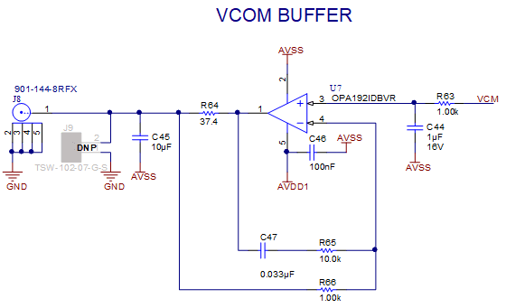
GUID-47FB65F9-4D9A-4AB2-B876-B25BB48B2591-low.gifFigure 2-3 VCOM Buffer