SBOA294 April 2021 OPA375 , TLV9001
Design Goals
| Input | Output | BW | Supply | |||
|---|---|---|---|---|---|---|
| ViMin | ViMax | VoMin | VoMax | fc | Vcc | Vee |
| –0.1V | 0.1V | –2V | 2V | 10kHz | 2.5V | –2.5V |
Design Description
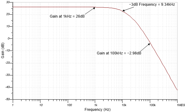
This low-pass non-inverting circuit amplifies the signal level by 20V/V (26dB) and filters the signal by setting the pole at 10kHz. Components R1 and C1 create a low-pass filter on the non-inverting pin. The frequency response of this circuit is the same as that of a passive RC filter, except that the output is amplified by the pass-band gain of the amplifier. Components C2 and R3 are used to set the cutoff frequency, fc, of the non-inverting amplifier.

Design Notes
- The common-mode voltage is equal to the input voltage applied to the non-inverting input of the op amp.
- Using high-value resistors can degrade the phase margin of the circuit and introduce additional noise in the circuit.
- Set the pole frequency created by R3 / C2 to be ten times higher than the pole created by R1 / C1 to achieve a single poll roll-off that is dominated by R1 / C1. If the filter pairs R1 / C1 and R3 / C2 have the same pole frequency, the gain will be reduced by 6dB at the cutoff frequency. Also the gain decreases at a rate of –40dB/dec until the response reaches 0dB, after which the slope changes to –20dB/dec until the op amp runs out of bandwidth.
- C2 limits the bandwidth of the non-inverting gain stage.
- Avoid placing capacitive loads directly on the output of the amplifier to minimize stability issues.
- Large signal performance may be limited by slew rate. Therefore, check the maximum output swing versus frequency plot in the data sheet to minimize slew-induced distortion.
- For more information on an op amp linear operating region, stability, slew-induced distortion, capacitive load drive, driving ADCs, and bandwidth, see the Design References section.
Design Steps
The DC transfer function of this circuit follows:
- Calculate the gain. Equation 1.
- Calculate values for R2 and R3. Equation 1.
Choose R2 = 1kΩ:
Equation 1. - Calculate the component values R1 and C1 to set the cutoff frequency, fc. Pick the value of R1 and then calculate C1 to set the location of fc.
Choose R1 = 1kΩ:
Equation 1. - Calculate C2 value to set the cutoff frequency (fc) of the op amp. Select the corner frequency to be at least ten times larger than fc. Equation 1.Equation 1.
Design Simulations
AC Simulation Results
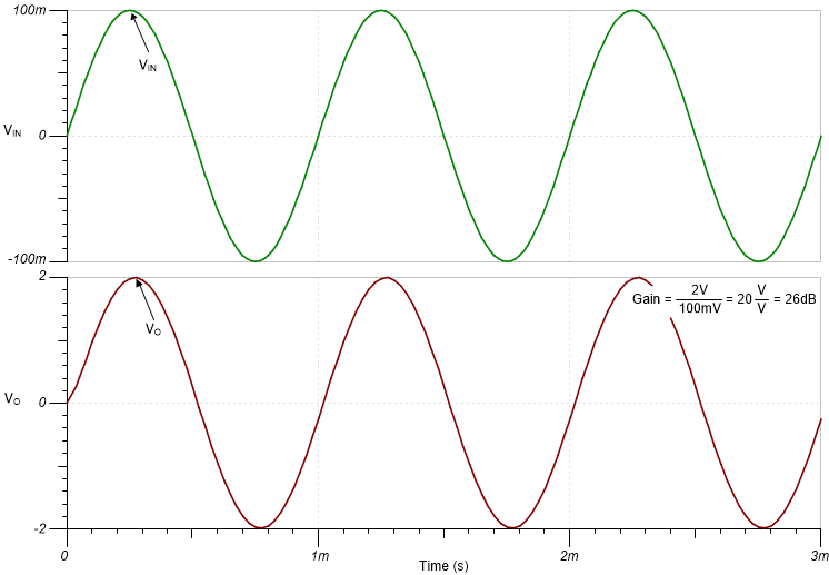
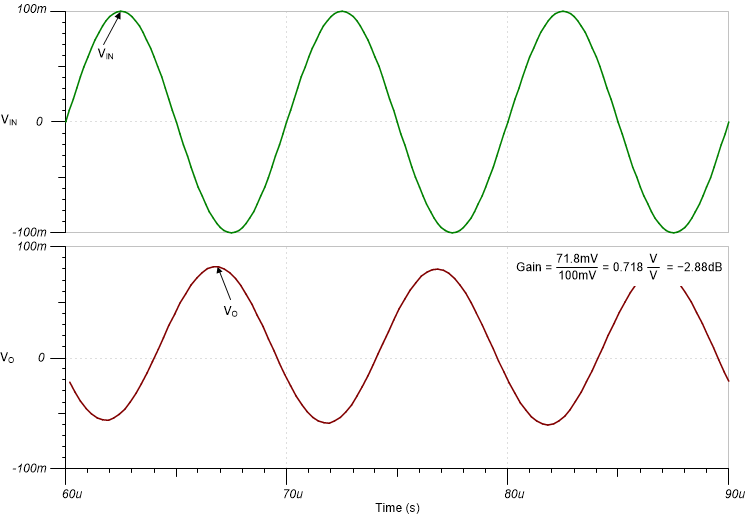
Transient Simulation Results
A 1-kHz, 0.2-VPP sine wave yields a 4-VPP output sine wave.
A 100-kHz, 0.2-VPP sine wave yields a 0.071-VPP output sine wave.
Design References
- See Analog Engineer's Circuit Cookbooks for the comprehensive TI circuit library.
- SPICE Simulation File SBOC528.
- TI Precision Labs
- See the AC Coupled, Single-Supply, Inverting and Non-inverting Amplifier Reference Design.
Design Featured Op Amp
| TLV9001 | |
|---|---|
| Vss | 1.8V to 5.5V |
| VinCM | Rail-to-rail |
| Vout | Rail-to-rail |
| Vos | 0.4mV |
| Iq | 60µA |
| Ib | 5pA |
| UGBW | 1MHz |
| SR | 2V/µs |
| #Channels | 1,2,4 |
| www.ti.com/product/TLV9001 | |
Design Alternate Op Amp
| OPA375 | |
|---|---|
| Vss | 2.25V to 5.5V |
| VinCM | Vee to Vcc – 1.2V |
| Vout | Rail-to-rail |
| Vos | 0.15mV |
| Iq | 890µA |
| Ib | 10pA |
| UGBW | 10MHz |
| SR | 4.75V/µs |
| #Channels | 1,2,4 |
| www.ti.com/product/OPA375 | |