SBOA345 June 2021 ADC10D1000QML-SP , ADC12D1600QML-SP , ADC12D1620QML-SP , INA1620 , OPA132 , OPA134 , OPA1602 , OPA1604 , OPA1611 , OPA1612 , OPA1622 , OPA1632 , OPA1637 , OPA1641 , OPA1642 , OPA1644 , OPA1652 , OPA1654 , OPA1655 , OPA1656 , OPA1662 , OPA1664 , OPA1671 , OPA1677 , OPA1678 , OPA1679 , OPA1688 , OPA1692 , OPA2132 , OPA2134 , OPA4132 , OPA4134
2 Operational Amplifier Voltage Noise
An operational amplifier has a voltage noise and current noise source. The magnitude of the noise sources inside the amplifier is given in the amplifier’s data sheet. When considering the voltage noise of an amplifier, it is important to realize the architecture of the amplifier. Typically, a bipolar input amplifier will have much lower voltage noise than a CMOS input amplifier for the same amount of quiescent current. For more information on the difference between amplifier architectures see this technical article: Trade-offs Between CMOS, JFET, and Bipolar Input Stage Technology. Before discussing the different types of voltage noise, it’s important to understand what this noise looks like in an amplifier circuit. Amplifier noise can be simplified by modeling it as an external voltage noise en(v) on the positive terminal of the amplifier as shown in Figure 2-1.
 Figure 2-1 Voltage Noise
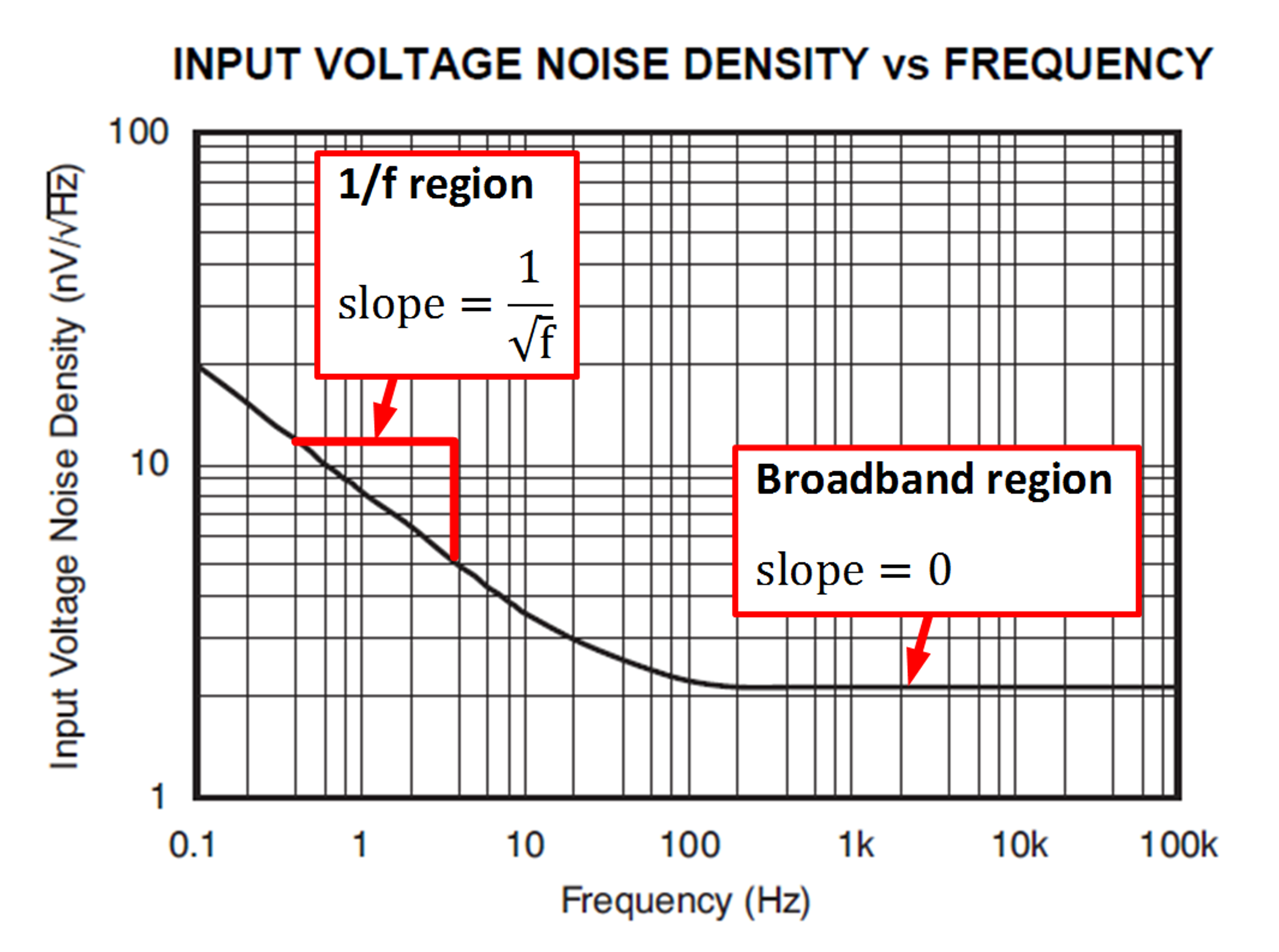
Amplifier voltage noise can be broken down into two main components: flicker noise and broadband noise. Figure 1-1 displays these noise regions.
 Figure 2-2 Voltage Noise Density
Curve