SCDA008C June 2021 – November 2021 CD4052B , TS3A225E , TS3A44159
- Trademarks
- 1Introduction
- 2Semiconductor Switches
- 3Basic Signal-Switch Structures
- 4Key Concerns in Digital-Switch Applications
- 5Signal Switch Families
- 6Applications
- 7Conclusion
- 8References
- 9Revision History
-
A Test
Measurement Circuits
- A.1 Measurement Setup for ron
- A.2 Measurement Setup for VO vs VI Characteristics
- A.3 Voltage-Time Waveform Measurement (Switch On)
- A.4 Voltage-Time Waveform Measurement (Switch Off)
- A.5 Output-Skew Measurement
- A.6 Simulation Setup for Undershoot Measurement
- A.7 Laboratory Setup for Attenuation Measurement
- A.8 Laboratory Setup for Off Isolation Measurement
- A.9 Laboratory Setup for Crosstalk Measurement
3.2 NMOS/PMOS Parallel Switch
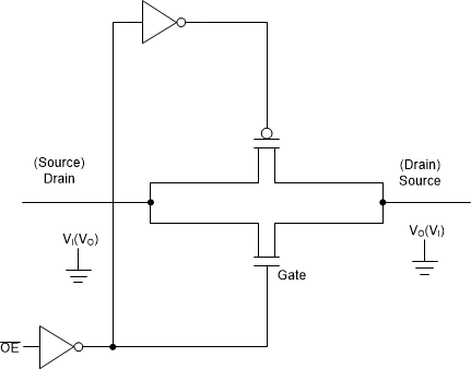
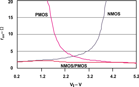
An NMOS/PMOS parallel switch consists of an n-channel pass transistor in parallel with ap-channel pass transistor. Figure 3-3 shows the basic structure of an NMOS/PMOS parallel switch. In an n-channel MOSFET, the source-to-drain resistance is low when the drain voltage is less than VG – VT, where VG is the gate voltage. In a p-channel MOSFET, the source-to-drain resistance is low when the source voltage is greater than VT + VG. with the parallel combination of n-channel and p-channel pass transistors, the source-to-drain, or channel resistance, can be lowered for the entire input voltage range from 0 V to VG. When OE is low, VG in NMOS/PMOS parallel switch is VCC, and signals ranging from 0 V to VCC can be passed through this switch. Figure 3-4 shows the general shape of the ron versus VI characteristics of a typical NMOS/PMOS parallel switch, as well as the NMOS and PMOS characteristics. The shape of ron vs VI curve may be different, depending on the structures of NMOS and PMOS. The disadvantage of the NMOS/PMOS parallel switch is that the input and output capacitances increase due to the additional source and drain area of the combined transistors.
 Figure 3-3 Basic Structure of an NMOS/PMOS Parallel Switch
 Figure 3-4 ron vs VI Characteristics of a Typical NMOS/PMOS Parallel Switch (VCC = 5 V)