SCDA008C June 2021 – November 2021 CD4052B , TS3A225E , TS3A44159
- Trademarks
- 1Introduction
- 2Semiconductor Switches
- 3Basic Signal-Switch Structures
- 4Key Concerns in Digital-Switch Applications
- 5Signal Switch Families
- 6Applications
- 7Conclusion
- 8References
- 9Revision History
-
A Test
Measurement Circuits
- A.1 Measurement Setup for ron
- A.2 Measurement Setup for VO vs VI Characteristics
- A.3 Voltage-Time Waveform Measurement (Switch On)
- A.4 Voltage-Time Waveform Measurement (Switch Off)
- A.5 Output-Skew Measurement
- A.6 Simulation Setup for Undershoot Measurement
- A.7 Laboratory Setup for Attenuation Measurement
- A.8 Laboratory Setup for Off Isolation Measurement
- A.9 Laboratory Setup for Crosstalk Measurement
5.3 CB3Q Family
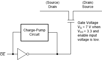
The switches of the CB3Q (High-Bandwidth Cross-Bar Technology) family are NMOS only, with a low and flat ron. The flat characteristics of ron are accomplished by a charge-pump circuit that generates a voltage of approximately 7 V at the gate of the n-channel pass transistor. As a result, 0-V to 5-V rail-to-rail switching can be accomplished because the gate-to-source voltage is well above the threshold of the n-channel transistor, and the switch is completely on over the whole 0-V to 5-V range. An internal oscillator circuit is a part of the charge-pump circuit; therefore, static power consumption of this family is higher than the CBT-C family. Dynamic power consumption depends on the frequency of the enable input. In addition to the low and flat ron characteristics, this family has low input and output capacitance, making them suitable for high-performance applications. The maximum switching frequency for I/O signals depends on various factors, such as type of load, input-signal magnitude, input-signal edge rates, type of package, and so forth with a larger package, the inductance and capacitance can form a resonant circuit that may cause phase and magnitude distortion. with a large capacitive load, the RC time constant becomes higher and limits the frequency. Figure 5-9 shows a simplified schematic of a CB3Q device.
 Figure 5-9 Simplified Schematic of a CB3Q device